Low Noise and Distortion,
Rail-to-Rail Output Amplifier
ADA4841-2KGD
Known Good Die
FEATURES
FUNCTIONAL BLOCK DIAGRAM
Low power: 1.1 mA/amplifier
Low wideband noise
2.1 nV/√Hz
1.4 pA/√Hz
Low 1/f noise
7 nV/√Hz at 10 Hz
13 pA/√Hz at 10 Hz
Low distortion: −105 dBc at 100 kHz, VO = 2 V p-p
High speed
80 MHz, −3 dB bandwidth (G = +1)
12 V/µs slew rate
175 ns settling time to 0.1%
Low offset voltage: 0.3 mV maximum
Rail-to-rail output
Wide supply range: 2.7 V to 12 V
Known good die (KGD): these die are fully guaranteed to
data sheet specifications
ADA4841-2KGD
OUT1
OUT2
+IN1
–IN2
–VS
+IN2
13370-001
+VS
–IN1
Figure 1.
APPLICATIONS
Low power, low noise signal processing
Battery-powered instrumentation
16-bit PulSAR® ADC drivers
GENERAL DESCRIPTION
The ADA4841-2KGD provides the performance required to
efficiently support emerging 16-bit to 18-bit ADCs and is ideal
for portable instrumentation, high channel count, industrial measurement, and medical applications. The ADA4841-2KGD is
ideally suited to drive the AD7685/AD7686, 16-bit PulSAR ADCs.
Rev. 0
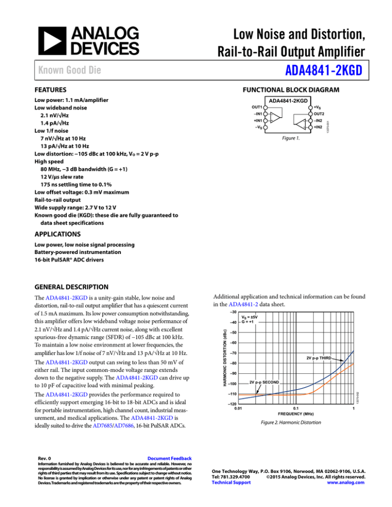
–30
–40
VS = ±5V
G = +1
–50
–60
–70
2V p-p THIRD
–80
–90
–100
2V p-p SECOND
13370-002
The ADA4841-2KGD output can swing to less than 50 mV of
either rail. The input common-mode voltage range extends
down to the negative supply. The ADA4841-2KGD can drive up
to 10 pF of capacitive load with minimal peaking.
Additional application and technical information can be found
in the ADA4841-2 data sheet.
HARMONIC DISTORTION (dBc)
The ADA4841-2KGD is a unity-gain stable, low noise and
distortion, rail-to-rail output amplifier that has a quiescent current
of 1.5 mA maximum. Its low power consumption notwithstanding,
this amplifier offers low wideband voltage noise performance of
2.1 nV/√Hz and 1.4 pA/√Hz current noise, along with excellent
spurious-free dynamic range (SFDR) of −105 dBc at 100 kHz.
To maintain a low noise environment at lower frequencies, the
amplifier has low 1/f noise of 7 nV/√Hz and 13 pA/√Hz at 10 Hz.
–110
–120
0.01
0.1
FREQUENCY (MHz)
1
Figure 2. Harmonic Distortion
Document Feedback
Information furnished by Analog Devices is believed to be accurate and reliable. However, no
responsibility isassumed by Analog Devices for itsuse, nor for any infringementsofpatentsor other
rights of third parties that may result from its use. Specifications subject to change without notice.
No license is granted by implication or otherwise under any patent or patent rights of Analog
Devices.Trademarks and registered trademarks are the property of their respective owners.
One Technology Way, P.O. Box 9106, Norwood, MA 02062-9106, U.S.A.
Tel: 781.329.4700
©2015 Analog Devices, Inc. All rights reserved.
Technical Support
www.analog.com
ADA4841-2KGD
Known Good Die
TABLE OF CONTENTS
Features .............................................................................................. 1
3 V Supply ......................................................................................5
Applications ....................................................................................... 1
Absolute Maximum Ratings ............................................................6
Functional Block Diagram .............................................................. 1
ESD Caution...................................................................................6
General Description ......................................................................... 1
Pin Configuration and Function Descriptions..............................7
Revision History ............................................................................... 2
Outline Dimensions ..........................................................................8
Specifications..................................................................................... 3
Die Specifications and Assembly Recommendations ..............8
±5 V Supply ................................................................................... 3
Ordering Guide .............................................................................8
5 V Supply...................................................................................... 4
REVISION HISTORY
9/15—Revision 0: Initial Version
Rev. 0 | Page 2 of 8
Known Good Die
ADA4841-2KGD
SPECIFICATIONS
±5 V SUPPLY
TA = 25°C, RL = 1 kΩ, G = +1, unless otherwise noted.
Table 1.
Parameter
DYNAMIC PERFORMANCE
−3 dB Bandwidth
Slew Rate
Settling Time to 0.1%
Settling Time to 0.01%
NOISE/HARMONIC PERFORMANCE
Harmonic Distortion HD2/HD3
Input Voltage Noise
Input Current Noise
DC PERFORMANCE
Input Offset Voltage
Input Offset Voltage Drift
Input Bias Current
Input Offset Current
Open-Loop Gain
INPUT CHARACTERISTICS
Input Resistance
Common Mode
Differential Mode
Input Capacitance
Common Mode
Differential Mode
Input Common-Mode Voltage Range
Common-Mode Rejection Ratio (CMRR)
MATCHING CHARACTERISTICS
Input Offset Voltage
Input Bias Current
OUTPUT CHARACTERISTICS
Output Voltage Swing
Output Current Limit
Capacitive Load Drive
POWER SUPPLY
Operating Range
Quiescent Current/Amplifier
Positive Power Supply Rejection Ratio
Negative Power Supply Rejection Ratio
Test Conditions/Comments
Min
Typ
Max
Unit
VO = 0.02 V p-p
VO = 2 V p-p
G = +1, VO = 9 V step, RL = 1 kΩ
G = +1, VO = 8 V step
G = +1, VO = 8 V step
80
3
13
650
1000
MHz
MHz
V/μs
ns
ns
fC = 100 kHz, VO = 2 V p-p, G = +1
fC = 1 MHz, VO = 2 V p-p
f = 100 kHz
f = 100 kHz
−111/−105
−80/−67
2.1
1.4
dBc
dBc
nV/√Hz
pA/√Hz
VO = ±4 V
40
1
3
0.1
120
VCM = Δ4 V
G > +1
Sourcing, VIN = +VS, RL = 50 Ω to GND
Sinking, VIN = −VS, RL = 50 Ω to GND
30% overshoot
103
−5.1
95
±4.9
Rev. 0 | Page 3 of 8
95
96
5.3
0.5
μV
μV/°C
μA
μA
dB
90
25
MΩ
kΩ
1
3
115
pF
pF
V
dB
70
60
μV
nA
±4.955
30
60
15
V
mA
mA
pF
+4
2.7
+VS = +5 V to +6 V, −VS = −5 V
+VS = +5 V, −VS = −5 V to −6 V
300
1.2
110
120
12
1.5
V
mA
dB
dB
ADA4841-2KGD
Known Good Die
5 V SUPPLY
TA = 25°C, RL = 1 kΩ, G = +1, VCM = 2.5 V, unless otherwise noted.
Table 2.
Parameter
DYNAMIC PERFORMANCE
−3 dB Bandwidth
Slew Rate
Settling Time to 0.1%
Settling Time to 0.01%
NOISE/HARMONIC PERFORMANCE
Harmonic Distortion HD2/HD3
Input Voltage Noise
Input Current Noise
Crosstalk
DC PERFORMANCE
Input Offset Voltage
Input Offset Voltage Drift
Input Bias Current
Input Offset Current
Open-Loop Gain
INPUT CHARACTERISTICS
Input Resistance
Common Mode
Differential Mode
Input Capacitance
Common Mode
Differential Mode
Input Common-Mode Voltage Range
Common-Mode Rejection Ratio (CMRR)
MATCHING CHARACTERISTICS
Input Offset Voltage
Input Bias Current
OUTPUT CHARACTERISTICS
Output Voltage Swing
Output Current Limit
Capacitive Load Drive
POWER SUPPLY
Operating Range
Quiescent Current/Amplifier
Positive Power Supply Rejection Ratio
Negative Power Supply Rejection Ratio
Test Conditions/Comments
Min
Typ
Max
Unit
VO = 0.02 V p-p
VO = 2 V p-p
G = +1, VO = 4 V step, RL = 1 kΩ
G = +1, VO = 2 V step
G = +1, VO = 2 V step
80
3
12
175
550
MHz
MHz
V/μs
ns
ns
fC = 100 kHz, VO = 2 V p-p
fC = 1 MHz, VO = 2 V p-p
f = 100 kHz
f = 100 kHz
f = 100 kHz
−109/−105
−78/−66
2.1
1.4
−117
dBc
dBc
nV/√Hz
pA/√Hz
dB
VO = 0.5 V to 4.5 V
40
1
3
0.1
124
103
−0.1
88
VCM = Δ1.5 V
G > +1
Sourcing, VIN = +VS, RL = 50 Ω to VCM
Sinking, VIN = −VS, RL = 50 Ω to VCM
30% overshoot
0.08 to 4.92
Rev. 0 | Page 4 of 8
95
96
5.3
0.4
μV
μV/°C
μA
μA
dB
90
25
MΩ
kΩ
1
3
115
pF
pF
V
dB
70
70
μV
nA
0.029 to 4.974
30
60
15
V
mA
mA
pF
+4
2.7
+VS = +5 V to +6 V, −VS = 0 V
+VS = +5 V, −VS = 0 V to −1 V
300
1.1
110
120
12
1.4
V
mA
dB
dB
Known Good Die
ADA4841-2KGD
3 V SUPPLY
TA = 25°C, RL = 1 kΩ, G =+1, VCM = 1.5 V, unless otherwise noted.
Table 3.
Parameter
DYNAMIC PERFORMANCE
−3 dB Bandwidth
Slew Rate
Settling Time to 0.1%
Settling Time to 0.01%
NOISE/HARMONIC PERFORMANCE
Harmonic Distortion HD2/HD3
Input Voltage Noise
Input Current Noise
DC PERFORMANCE
Input Offset Voltage
Input Offset Voltage Drift
Input Bias Current
Input Offset Current
Open-Loop Gain
INPUT CHARACTERISTICS
Input Resistance
Common Mode
Differential Mode
Input Capacitance
Common Mode
Differential Mode
Input Common-Mode Voltage Range
Common-Mode Rejection Ratio (CMRR)
MATCHING CHARACTERISTICS
Input Offset Voltage
Input Bias Current
OUTPUT CHARACTERISTICS
Output Voltage Swing
Output Current Limit
Capacitive Load Drive
POWER SUPPLY
Operating Range
Quiescent Current/Amplifier
Positive Power Supply Rejection Ratio
Negative Power Supply Rejection Ratio
Test Conditions/Comments
Min
Typ
Max
Unit
VO = 0.02 V p-p
G = +1, VO = 2 V step, RL = 1 kΩ
G = +1, VO = 1 V step
G = +1, VO = 1 V step
80
12
120
250
MHz
V/μs
ns
ns
fC = 100 kHz, VO = 1 V p-p
fC = 1 MHz, VO = 1 V p-p
f = 100 kHz
f = 100 kHz
−97/−100
−79/−80
2.1
1.4
dBc
dBc
nV/√Hz
pA/√Hz
VO = 0.5 V to 2.5 V
40
1
3
0.1
123
101
−0.1
86
VCM = Δ0.4 V
G > +1
Sourcing, VIN = +VS, RL = 50 Ω to VCM
Sinking, VIN = −VS, RL = 50 Ω to VCM
30% overshoot
0.045 to 2.955
Rev. 0 | Page 5 of 8
95
96
5.3
0.5
μV
μV/°C
μA
μA
dB
90
25
MΩ
kΩ
1
3
115
pF
pF
V
dB
70
60
μV
nA
0.023 to 2.988
30
60
30
V
mA
mA
pF
+2
2.7
+VS = +3 V to +4 V, −VS = 0 V
+VS = +3 V, −VS = 0 V to −1 V
300
1.1
110
120
12
1.3
V
mA
dB
dB
ADA4841-2KGD
Known Good Die
ABSOLUTE MAXIMUM RATINGS
ESD CAUTION
Table 4.
Parameter
Supply Voltage
Common-Mode Input Voltage
Differential Input Voltage
Storage Temperature Range
Junction Temperature
Rating
12.6 V
−VS − 0.5 V to +VS + 0.5 V
±1.8 V
−65°C to +125°C
150°C
Stresses at or above those listed under Absolute Maximum
Ratings may cause permanent damage to the product. This is a
stress rating only; functional operation of the product at these
or any other conditions above those indicated in the operational
section of this specification is not implied. Operation beyond
the maximum operating conditions for extended periods may
affect product reliability.
Rev. 0 | Page 6 of 8
Known Good Die
ADA4841-2KGD
PIN CONFIGURATION AND FUNCTION DESCRIPTIONS
OUT1
1A
–IN1
1B
+VS
8A
8B
OUT2
7
2
ADA4841-2KGD
+IN1
3
4A
4B
–VS
6
–IN2
5
+IN2
13370-003
TOP VIEW
(Not to Scale)
Figure 3. Pad Configuration
Table 5. Pad Function Descriptions
Pad No.
1A,1B
2
3
4A, 4B
5
6
7
8A, 8B
X-Axis
−463, −393
−597
−597
−36, +35
+603
+603
+568
−36, +35
Y-Axis
+363
+334
−250
−363
−363
−245
+363
+363
Mnemonic
OUT1
−IN1
+IN1
−VS
+IN2
−IN2
OUT2
+VS
Rev. 0 | Page 7 of 8
Description
Output 1, Double Bond Pad
Inverting Input 1
Noninverting Input 1
Negative Supply, Double Bond Pad
Noninverting Input 2
Inverting Input 2
Output 2
Positive Supply, Double Bond Pad
ADA4841-2KGD
Known Good Die
OUTLINE DIMENSIONS
1.525
1A
1B
8A
0.305
8B
7
2
0.940
4A
0.070 × 0.140
5
4B
TOP VIEW
0.070 × 0.070
(CIRCUIT SIDE)
SIDE VIEW
09-17-2015-A
6
3
Figure 4. 8-Pad Bare Die [CHIP]
(C-8-4)
Dimensions shown in millimeters
DIE SPECIFICATIONS AND ASSEMBLY RECOMMENDATIONS
Table 6. Die Specifications
Parameter
Scribe Line Width
Die Size (Maximum Size)
Thickness
Bond Pads (Minimum Size)
Bond Pad Composition
Backside
Passivation
ESD, Human Body Model (HBM)
Value
75
1525 × 940
305
70 × 70
0.5% AlCu
SOI
Doped-oxide/SiN
2000
Unit
μm
μm
μm
μm
%
Not applicable
Not applicable
V
Table 7. Assembly Recommendations
Assembly Component
Die Attach
Bonding Method
Recommendation
Ablestik 84-1LMIS R4
1 mil gold
ORDERING GUIDE
Model
ADA4841-2KGD-WP
Temperature Range
–40°C to +125°C
Package Description
8-Pad Bare Die [CHIP]
©2015 Analog Devices, Inc. All rights reserved. Trademarks and
registered trademarks are the property of their respective owners.
D13370-0-9/15(0)
Rev. 0 | Page 8 of 8
Package Option
C-8-4
Mouser Electronics
Authorized Distributor
Click to View Pricing, Inventory, Delivery & Lifecycle Information:
Analog Devices Inc.:
ADA4841-2YRMZ ADA4841-2YRZ ADA4841-2YCPZ-R7 ADA4841-2YRMZ-R7 ADA4841-2YRMZ-RL ADA48412YRZ-R7 ADA4841-2YRZ-RL ADA4841-2YCPZ-R2 ADA4841-2YCPZ-RL


