Terahertz photoconductivity of mobile electrons in nanoporous InP honeycombs * J. Lloyd-Hughes,
advertisement
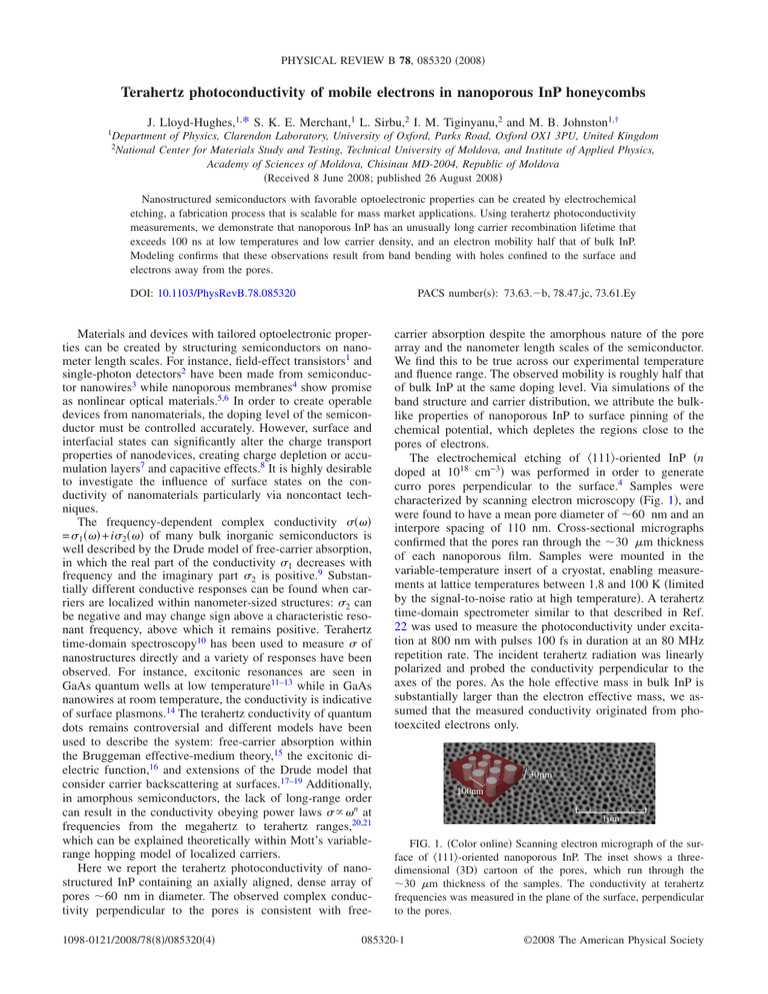
PHYSICAL REVIEW B 78, 085320 共2008兲 Terahertz photoconductivity of mobile electrons in nanoporous InP honeycombs J. Lloyd-Hughes,1,* S. K. E. Merchant,1 L. Sirbu,2 I. M. Tiginyanu,2 and M. B. Johnston1,† 1Department 2National of Physics, Clarendon Laboratory, University of Oxford, Parks Road, Oxford OX1 3PU, United Kingdom Center for Materials Study and Testing, Technical University of Moldova, and Institute of Applied Physics, Academy of Sciences of Moldova, Chisinau MD-2004, Republic of Moldova 共Received 8 June 2008; published 26 August 2008兲 Nanostructured semiconductors with favorable optoelectronic properties can be created by electrochemical etching, a fabrication process that is scalable for mass market applications. Using terahertz photoconductivity measurements, we demonstrate that nanoporous InP has an unusually long carrier recombination lifetime that exceeds 100 ns at low temperatures and low carrier density, and an electron mobility half that of bulk InP. Modeling confirms that these observations result from band bending with holes confined to the surface and electrons away from the pores. DOI: 10.1103/PhysRevB.78.085320 PACS number共s兲: 73.63.⫺b, 78.47.jc, 73.61.Ey Materials and devices with tailored optoelectronic properties can be created by structuring semiconductors on nanometer length scales. For instance, field-effect transistors1 and single-photon detectors2 have been made from semiconductor nanowires3 while nanoporous membranes4 show promise as nonlinear optical materials.5,6 In order to create operable devices from nanomaterials, the doping level of the semiconductor must be controlled accurately. However, surface and interfacial states can significantly alter the charge transport properties of nanodevices, creating charge depletion or accumulation layers7 and capacitive effects.8 It is highly desirable to investigate the influence of surface states on the conductivity of nanomaterials particularly via noncontact techniques. The frequency-dependent complex conductivity 共兲 = 1共兲 + i2共兲 of many bulk inorganic semiconductors is well described by the Drude model of free-carrier absorption, in which the real part of the conductivity 1 decreases with frequency and the imaginary part 2 is positive.9 Substantially different conductive responses can be found when carriers are localized within nanometer-sized structures: 2 can be negative and may change sign above a characteristic resonant frequency, above which it remains positive. Terahertz time-domain spectroscopy10 has been used to measure of nanostructures directly and a variety of responses have been observed. For instance, excitonic resonances are seen in GaAs quantum wells at low temperature11–13 while in GaAs nanowires at room temperature, the conductivity is indicative of surface plasmons.14 The terahertz conductivity of quantum dots remains controversial and different models have been used to describe the system: free-carrier absorption within the Bruggeman effective-medium theory,15 the excitonic dielectric function,16 and extensions of the Drude model that consider carrier backscattering at surfaces.17–19 Additionally, in amorphous semiconductors, the lack of long-range order can result in the conductivity obeying power laws ⬀ n at frequencies from the megahertz to terahertz ranges,20,21 which can be explained theoretically within Mott’s variablerange hopping model of localized carriers. Here we report the terahertz photoconductivity of nanostructured InP containing an axially aligned, dense array of pores ⬃60 nm in diameter. The observed complex conductivity perpendicular to the pores is consistent with free1098-0121/2008/78共8兲/085320共4兲 carrier absorption despite the amorphous nature of the pore array and the nanometer length scales of the semiconductor. We find this to be true across our experimental temperature and fluence range. The observed mobility is roughly half that of bulk InP at the same doping level. Via simulations of the band structure and carrier distribution, we attribute the bulklike properties of nanoporous InP to surface pinning of the chemical potential, which depletes the regions close to the pores of electrons. The electrochemical etching of 具111典-oriented InP 共n doped at 1018 cm−3兲 was performed in order to generate curro pores perpendicular to the surface.4 Samples were characterized by scanning electron microscopy 共Fig. 1兲, and were found to have a mean pore diameter of ⬃60 nm and an interpore spacing of 110 nm. Cross-sectional micrographs confirmed that the pores ran through the ⬃30 m thickness of each nanoporous film. Samples were mounted in the variable-temperature insert of a cryostat, enabling measurements at lattice temperatures between 1.8 and 100 K 共limited by the signal-to-noise ratio at high temperature兲. A terahertz time-domain spectrometer similar to that described in Ref. 22 was used to measure the photoconductivity under excitation at 800 nm with pulses 100 fs in duration at an 80 MHz repetition rate. The incident terahertz radiation was linearly polarized and probed the conductivity perpendicular to the axes of the pores. As the hole effective mass in bulk InP is substantially larger than the electron effective mass, we assumed that the measured conductivity originated from photoexcited electrons only. FIG. 1. 共Color online兲 Scanning electron micrograph of the surface of 具111典-oriented nanoporous InP. The inset shows a threedimensional 共3D兲 cartoon of the pores, which run through the ⬃30 m thickness of the samples. The conductivity at terahertz frequencies was measured in the plane of the surface, perpendicular to the pores. 085320-1 ©2008 The American Physical Society PHYSICAL REVIEW B 78, 085320 共2008兲 LLOYD-HUGHES et al. −1 Im[σ] (Ω cm ) 80 40 20 6.2 n 14 10 (c) 13 10 0 1 2 Frequency ω/2π (THz) 0 of frequency in the Drude model. It can be seen readily from Eq. 共2兲 that ⌫ is given by (b) 0 40 3.7 n0 ⌫= 2 n0 1 n0 0 0 1 2 Frequency ω/2π (THz) 1 0.6 0.8 0.4 0.6 (d) 0.4 0.2 0.2 0 0 0 5 10 15 Fluence n/n0 N (1017cm−3) −1 12 n 20 0 0 1 2 Frequency ω/2π (THz) Γ(ω) (s ) 60 −1 60 (a) τ (µs) Re[σ] (Ω−1cm−1) 80 FIG. 2. 共Color online兲 关共a兲 and 共b兲兴 Shaded areas show the measured 共a兲 real and 共b兲 imaginary parts of the photoexcited conductivity of nanoporous InP at a lattice temperature of 40 K at various incident fluences ranging from n0 = 6.0⫻ 1010 cm−2 to 12n0. Solid lines are fits using the Drude conductivity of a free-electron gas 关Eq. 共2兲兴. 共c兲 ⌫共兲 calculated from Eq. 共3兲 at fluences of n0 共points兲 and 12n0 共crosses兲. 共d兲 Electron density extracted from the fits to the Drude conductivity 共circles兲 and calculated carrier lifetime −0.77 共squares兲. The solid line 共N ⬀ n0.23 兲 are 0 兲 and dashed line 共 ⬀ n0 guides to the eye. The measured conductivity was not observed to alter with pump-probe delay time both before and after the arrival of the pump pulse at “zero delay.” This suggests that the carrier recombination lifetime in nanoporous InP is long in comparison to the laser repetition period 共⌬t = 12.5 ns兲. In the limit Ⰷ ⌬t, a simple rate equation yields the equilibrated photoinduced charge density N as N = N0 , ⌬t 共1兲 where N0 is the carrier density generated by a single pulse. The photoexcited carrier density can therefore be enhanced substantially above N0, depending on . We calculated N0 at each pump fluence from the measured pump spot size, power, and absorption depth at 800 nm of InP. Equation 共1兲 is used later to calculate from N determined from the frequency-dependent conductivity. In Figs. 2共a兲 and 2共b兲 the real and imaginary parts of the photoconductivity are plotted at various incident pump fluences for a lattice temperature of 40 K. Considering the data at the lowest fluence 共bottom shaded areas兲, 1 is positive throughout the frequency range and decreases weakly with frequency. The imaginary part of is positive and increases with frequency. These trends are reproduced well by the Drude model of free electrons, as shown by the solid lines. In this model the complex conductivity can be written as 共兲 = Ne2共i + ⌫兲 , m ⴱ共 2 + ⌫ 2兲 共2兲 where N, e, and mⴱ are, respectively, the density, charge, and effective mass of electrons in the material 共we assume that mⴱ = 0.08me, the bulk value for InP兲. ⌫ is the electron momentum scattering rate, which is assumed to be independent 1共 兲 . 2共 兲 共3兲 This means that the electron momentum scattering rate can be calculated directly as a function of frequency from the experimental 共兲. Any frequency dependence to ⌫共兲 would immediately invalidate the Drude approach. In Fig. 2共c兲 ⌫共兲 is shown as calculated from the experimental 共兲 using Eq. 共3兲 at the lowest and highest fluence. No frequency dependence to ⌫ can be resolved, indicating the validity of the Drude approach, and the scattering rate is also independent of pump fluence. The obtained value of ⌫ = 2.7⫻ 1013 s−1 corresponds to an electron mobility ⯝ 814 cm2 V−1 s−1, almost half that of bulk InP 共 ⬃ 2000 cm2 V−1 s−1兲 at a similar doping level and temperature.23 The corresponding mean-free path for electrons is 6 nm, smaller than the narrowest width of the semiconductor honeycomb 共⬃50 nm兲, and thus surface scattering only weakly affects the mobility. This finding is consistent with the high mobility of GaAs nanowires recently reported.14 At high pump-laser fluence the spectral shape of the conductivity remains similar to that at low fluence 关Figs. 2共a兲 and 2共b兲兴. The change in the photoexcited electron density N with pump fluence n is shown in Fig. 2共d兲, as obtained from fits using Eq. 共2兲, with the value of ⌫ fixed to that in Fig. 2共c兲. We also calculate the recombination lifetime at each pump fluence from the fitted N using Eq. 共1兲. At low fluence, ⬃ 400 ns, a value much longer than that which we directly measure for bulk InP 共300 ps兲. Larger recombination times are often seen when electron-hole recombination is suppressed by charge separation, for instance, in nipi superlattices.24 The photoexcited electron density N increases sublinearly with fluence, which can be attributed to a reduction in due to an enhanced electron recombination rate. The origin of this effect is discussed below in conjunction with a simulation of the material’s electronic structure. Furthermore, we have measured the conductivity of nanoporous InP at lattice temperatures from 1.8 up to 100 K 共limited by the obtainable signal兲. The frequency dependence of is consistent with the Drude conductivity over this temperature range. In Fig. 3 we show the momentum scattering time 1 / ⌫ 关obtained from Eq. 共3兲兴 as a function of temperature. At higher lattice temperatures the mobility = e / 共⌫mⴱ兲 decreases slightly, ruling out a thermally activated transport mechanism such as the two-dimensional 共2D兲 variable-range hopping relation ⬀ exp关共T0 / T兲−1/3兴.25 This is further evidence that the nanoscale pores do not appear to hinder bulklike semiconductor transport. As a comparison, the scattering time for bulk 1018 cm−3 n-type InP is also plotted in Fig. 3, taken from Hall mobility measurements.23 The scattering rate for bulk InP is also not strongly temperature dependent as a result of carrierimpurity scattering dominating the mobility.23 In contrast, the scattering time for semi-insulating InP 共circles兲 displays a peak in 1 / ⌫ at 80 K. This is a characteristic of less heavily doped polar semiconductors when at high tem- 085320-2 PHYSICAL REVIEW B 78, 085320 共2008兲 1 10 1/Γ (s) −3 17 2 10 50 0 0 10 0.5 0 −0.5 −1 −1.5 0 E (eV) τ (ns) 100 (b) 1 10 Temperature (K) 2 10 (a) 200 100 x (nm) 100 200 0 300 (c) 0.5 0 −0.5 −1 0 (d) (b) 100 200 x (nm) 300 220 230 240 250 x (nm) 1 0.5 0 N (arb. units) 0 1 0.8 0.6 0.4 0.2 0 Ne (10 cm ) nanoporous InP −14 10 n InP (a) −13 10 10 + 300 ρ (1016cm−3) semi−insulating InP −12 10 y (nm) TERAHERTZ PHOTOCONDUCTIVITY OF MOBILE… FIG. 3. 共Color online兲 共a兲 The temperature dependence of the carrier momentum scattering time 1 / ⌫ is shown at an incident fluence of 12n0 for nanoporous InP 共squares兲 and bulk n-type InP at a comparable doping level 共crosses, from Hall mobilities in Ref. 23兲. Also shown is 1 / ⌫ measured for semi-insulating InP 共circles兲. The dashed line indicates the temperature dependence of the mobility from TO-phonon scattering, ⬀ T−3/2. 共b兲 The recombination lifetime of photoexcited carriers in nanoporous InP 共crosses兲, obtained from Eq. 共1兲, utilizing fits to the complex conductivity as in Fig. 2共d兲. The value of at 296 K 共diamond兲 was measured under photoexcitation using pulses from an amplified laser 共Ref. 26兲. FIG. 4. 共Color online兲 Carrier density of nanoporous InP at 100 K, simulated as described in the text. 共a兲 Electron density without photoexcitation over a 300⫻ 300 nm2 area. The electron density is depleted close to the pores 共white circles兲. The horizontal dotted line indicates the cross section taken in the plot of the band structure 共b兲, in which the conduction and valence bands are shown relative to the Fermi level 共E = 0兲. 共c兲 Charge density under photoexcitation at ⌬N = 1017 cm−3. The negative regions away from the pores represent higher electron density; the solid line shows a conductive pathway. 共d兲 Normalized photoinduced change in electron density in a region along the cross section at ⌬N = 1016, 1017, and 1018 cm−3 共from inner to outer lines兲. peratures carrier-phonon scattering 共 ⬀ T−3/2, dashed line兲 dominates.27 In order to investigate the nanoscale physics of porous semiconductors theoretically, we used a self-consistent Schrödinger-Poisson solver28 to calculate the twodimensional carrier density and band structure in thermal equilibrium at 100 K. We used an n-type doping of 1.0 ⫻ 1018 cm−3 throughout the nanoporous material with a donor level of 6 meV below the conduction band.29 At the semiconductor surface, we assumed that the Fermi level was pinned 0.3 eV above its value in bulk, a typical value for InP surfaces.30 One-dimensional solutions to the SchrödingerPoisson equation indicated that the electron density was at most 4% different from that obtained upon neglecting quantum effects and, therefore in our 2D simulations, we solved the Poisson equation only. To represent the actual structure 共Fig. 1兲, we modeled the pores as a pseudorandom array of circles with mean diameter of 60 nm and interpore spacing of 110 nm, shown by the white circles in Fig. 4. The simulated electron density and band structure of nanoporous InP are shown in Figs. 4共a兲 and 4共b兲. The equilibrium electron density can be seen to be strongly depleted close to the pores 共white circles兲. This results from the pinning of the Fermi level at the surface, which bends the electronic bands upward, as Fig. 4共b兲 illustrates for a cross section through the pores. Within ⬃20 nm of the pores, the conduction band is raised higher above the chemical potential 共at 0 eV in this figure兲, creating an electron depletion layer. The spacing between pores is often comparable to the depletion width, resulting in the large depletion regions seen in Fig. 4共a兲. This electron depletion accounts for the good terahertz transmission through our nanoporous InP samples, which would otherwise be opaque owing to the 1018 cm−3 n-doping concentration and ⬃30 m thickness. Substantial electron density can occur only in regions where the nearest pore is at a distance greater than approximately 20 nm. In our simulation we introduced an extra donor density ⌬N = 1017 cm−3 in order to model the effect of photoexcitation in nanoporous InP. The immobile ionized donors are analogous to the low-mobility photogenerated hole population. In Fig. 4共c兲 the difference in charge density between this simulation and the equilibrium charge density is shown. Photoexcited electrons reside in the regions of large negative charge density, away from the pores, while excess positive charge is seen around the pores. Pathways for electrical conduction can be seen along regions where the pores are further separated, as indicated by the solid line in Fig. 4共c兲. The maximum photoinduced electron density is of the order of 1016 cm−3, as a result of the strong electron depletion regions. The electronic structure reported in Fig. 4 can account for the observed features of the terahertz-frequency photoconductivity. The regions of high electron density 关⬃20 nm, Fig. 4共d兲兴 are larger than the mean-free path 共7 nm at 100 K兲, and the conductivity should therefore have a frequency and temperature dependence similar to that of free electrons in bulk InP, as indeed we observed 共Figs. 2 and 3兲. Photoexcited electrons and holes are separated spatially, as the charge density in Fig. 4共c兲 indicates, which reduces radiative recombination and accounts for the long lifetimes reported herein. We performed simulations at different photoinjected carrier densities and plot the obtained photoinduced electron density in Fig. 4共d兲 for a region of the porous material. At ⌬N = 1018 cm−3 the maximum photoinduced electron density was 1017 cm−3, comparable to the experimental density 关Fig. 2共d兲兴. Increasing ⌬N from 1016 to 1018 cm−3 makes the electron distribution broader as a result of a flattening of the conduction band. This enhances the overlap of the electron and hole wave functions, creating a larger radiative recombination rate and reducing the recombination lifetime . This effect qualitatively explains the shortening in at higher pump-laser fluence shown in Fig. 2. 085320-3 PHYSICAL REVIEW B 78, 085320 共2008兲 LLOYD-HUGHES et al. The measured temperature dependence of is also shown in Fig. 3 and was obtained as described above with reference to Fig. 2共d兲. Toward higher temperatures, can be seen to decrease, which can be interpreted as follows. At low temperatures the photoexcited holes are confined close to the surface, the electron-hole separation is large, and the radiative recombination rate is therefore low. At higher temperatures, holes obtain sufficient thermal energy to escape the surface, increasing the recombination rate. Finally, the regions of electrostatically confined electrons are small enough to generate quantum confinement effects, which can enhance the binding energy of excitons. However, no excitonic resonance in the conductivity was observed here, in contrast to previous spectroscopic studies of other nanostructures, for instance GaAs quantum wells.31 This may be a result of our measurement technique averaging over regions with different sizes and therefore binding energies: *Present address: ETH Zürich, Institute for Quantum Electronics, Wolfgang-Pauli-Strasse 16, 8093 Zürich, Switzerland. james.lloyd-hughes@phys.ethz.ch †m.johnston@physics.ox.ac.uk 1 Y. Cui, Z. H. Zhong, D. L. Wang, W. U. Wang, and C. M. Lieber, Nano Lett. 3, 149 共2003兲. 2 A. Fujiwara, K. Yamazaki, and Y. Takahashi, Appl. Phys. Lett. 80, 4567 共2002兲. 3 M. Law, J. Goldberger, and P. D. Yang, Annu. Rev. Mater. Res. 34, 83 共2004兲. 4 H. Föll, S. Langa, J. Carstensen, M. Christophersen, and I. M. Tiginyanu, Adv. Mater. 共Weinheim, Ger.兲 15, 183 共2003兲. 5 I. M. Tiginyanu, I. V. Kravetsky, J. Monecke, W. Cordts, G. Marowsky, and H. L. Hartnagel, Appl. Phys. Lett. 77, 2415 共2000兲. 6 M. Reid, I. Cravetchi, R. Fedosejevs, I. M. Tiginyanu, L. Sirbu, and R. W. Boyd, Phys. Rev. B 71, 081306共R兲 共2005兲. 7 K. I. Seo, S. Sharma, A. A. Yasseri, D. R. Stewart, and T. I. Kamins, Electrochem. Solid-State Lett. 9, G69 共2006兲. 8 S. A. Dayeh, C. Soci, P. K. L. Yu, E. T. Yu, and D. L. Wang, Appl. Phys. Lett. 90, 162112 共2007兲. 9 D. Grischkowsky, S. Keiding, M. van Exter, and C. Fattinger, J. Opt. Soc. Am. B 7, 2006 共1990兲. 10 C. A. Schmuttenmaer, Chem. Rev. 共Washington, D.C.兲 104, 1759 共2004兲. 11 R. H. M. Groeneveld and D. Grischkowsky, J. Opt. Soc. Am. B 11, 2502 共1994兲. 12 R. A. Kaindl, M. A. Carnahan, D. Hagele, R. Lovenich, and D. S. Chemla, Nature 共London兲 423, 734 共2003兲. 13 J. Lloyd-Hughes, H. E. Beere, D. A. Ritchie, and M. B. Johnston, Phys. Rev. B 77, 125322 共2008兲. 14 P. Parkinson, J. Lloyd-Hughes, Q. Gao, H. H. Tan, C. Jagadish, M. B. Johnston, and L. M. Herz, Nano Lett. 7, 2162 共2007兲. 15 M. C. Beard, G. M. Turner, and C. A. Schmuttenmaer, Nano the excitonic oscillator strength would then be dispersed spectrally. We have reported herein that photoexcited nanoporous InP exhibits the frequency- and temperature-dependent conductivities of a free-electron gas with a mobility approaching that of bulk InP but a substantially longer carrier lifetime. Via two-dimensional simulations, we attribute this to charge separation within the nanoporous structure. Our findings highlight the important influence that surface states have on conduction in nanoscale semiconductors. The precise control of surface states is likely to be critical to the functionality of nanoelectronic devices. The authors would like to acknowledge financial support from the EPSRC-GB 共UK兲 and from INTAS under Grant No. 05–104–7567. Lett. 2, 983 共2002兲. Wang, J. Shan, M. A. Islam, I. P. Herman, M. Bonn, and T. F. Heinz, Nat. Mater. 5, 861 共2006兲. 17 N. V. Smith, Phys. Rev. B 64, 155106 共2001兲. 18 G. M. Turner, M. C. Beard, and C. A. Schmuttenmaer, J. Phys. Chem. B 106, 11716 共2002兲. 19 D. G. Cooke, A. N. MacDonald, A. Hryciw, J. Wang, Q. Li, A. Meldrum, and F. A. Hegmann, Phys. Rev. B 73, 193311 共2006兲. 20 P. Lunkenheimer and A. Loidl, Phys. Rev. Lett. 91, 207601 共2003兲. 21 H. Harimochi, J. Kitagawa, M. Ishizaka, Y. Kadoya, M. Yamanishi, S. Matsuishi, and H. Hosono, Phys. Rev. B 70, 193104 共2004兲. 22 J. Lloyd-Hughes, S. K. E. Merchant, L. Fu, H. H. Tan, C. Jagadish, E. Castro-Camus, and M. B. Johnston, Appl. Phys. Lett. 89, 232102 共2006兲. 23 W. Walukiewicz, J. Lagowski, L. Jastrzebski, P. Rava, M. Lichtensteiger, C. H. Gatos, and H. C. Gatos, J. Appl. Phys. 51, 2659 共1980兲. 24 M. B. Johnston, M. Gal, G. Li, and C. Jagadish, J. Appl. Phys. 82, 5748 共1997兲. 25 N. Mott, Rev. Mod. Phys. 50, 203 共1978兲. 26 S. K. E. Merchant, J. Lloyd-Hughes, L. Sirbu, I. M. Tiginyanu, P. Parkinson, L. M. Herz, and M. B. Johnston, Nanotechnology 19, 395704 共2008兲. 27 P. Y. Yu and M. Cardona, Fundamentals of Semiconductors, 3rd ed. 共Springer, New York, 2003兲. 28 NEXTNANO, http://www.wsi.tum.de/nextnano3/ 29 Handbook Series on Semiconductor Parameters 共World Scientific, Singapore, 1996兲, Chap. 7. 30 J. S. Hwang, W. Y. Chou, M. C. Hung, J. S. Wang, and H. H. Lin, J. Appl. Phys. 82, 3888 共1997兲. 31 B. Gerlach, J. Wusthoff, M. O. Dzero, and M. A. Smondyrev, Phys. Rev. B 58, 10568 共1998兲. 16 F. 085320-4
