AN-1238
APPLICATION NOTE
One Technology Way • P.O. Box 9106 • Norwood, MA 02062-9106, U.S.A. • Tel: 781.329.4700 • Fax: 781.461.3113 • www.analog.com
High Accuracy, Bipolar Voltage Output Digital-to-Analog Conversion Using the
AD5765 DAC
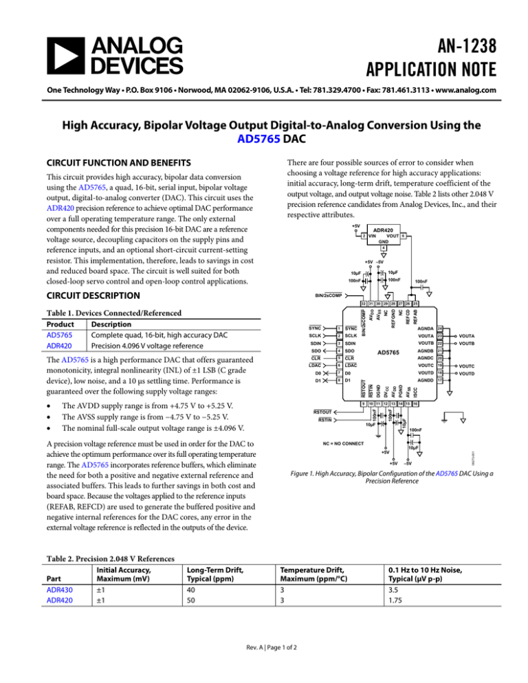
CIRCUIT FUNCTION AND BENEFITS
This circuit provides high accuracy, bipolar data conversion
using the AD5765, a quad, 16-bit, serial input, bipolar voltage
output, digital-to-analog converter (DAC). This circuit uses the
ADR420 precision reference to achieve optimal DAC performance
over a full operating temperature range. The only external
components needed for this precision 16-bit DAC are a reference
voltage source, decoupling capacitors on the supply pins and
reference inputs, and an optional short-circuit current-setting
resistor. This implementation, therefore, leads to savings in cost
and reduced board space. The circuit is well suited for both
closed-loop servo control and open-loop control applications.
There are four possible sources of error to consider when
choosing a voltage reference for high accuracy applications:
initial accuracy, long-term drift, temperature coefficient of the
output voltage, and output voltage noise. Table 2 lists other 2.048 V
precision reference candidates from Analog Devices, Inc., and their
respective attributes.
+5V
ADR420
2
VOUT 6
GND
VIN
4
+5V –5V
CIRCUIT DESCRIPTION
10µF
10µF
100nF
100nF
100nF
BIN/2sCOMP
SDIN
3
SDIN
SDO
4
SDO
REFAB
NC
REFCD
NC
AVSS
AVDD
REFGND
SCLK
AGNDA 24
VOUTA 23
VOUTA
VOUTB 22
VOUTB
AGNDB 21
AD5765
CLR
5
CLR
AGNDC 20
LDAC
6
LDAC
VOUTC 19
VOUTC
D0
7
D0
VOUTD 18
VOUTD
D1
8
D1
AGNDD 17
RSTIN
10µF
ISCC
AVSS
PGND
AVDD
DVCC
10 11 12 13 14 15 16
DGND
9
RSTOUT
10µF
The AVDD supply range is from +4.75 V to +5.25 V.
The AVSS supply range is from −4.75 V to −5.25 V.
The nominal full-scale output voltage range is ±4.096 V.
SYNC
2
100nF
100nF
A precision voltage reference must be used in order for the DAC to
achieve the optimum performance over its full operating temperature
range. The AD5765 incorporates reference buffers, which eliminate
the need for both a positive and negative external reference and
associated buffers. This leads to further savings in both cost and
board space. Because the voltages applied to the reference inputs
(REFAB, REFCD) are used to generate the buffered positive and
negative internal references for the DAC cores, any error in the
external voltage reference is reflected in the outputs of the device.
NC = NO CONNECT
10µF
+5V
+5V
–5V
Figure 1. High Accuracy, Bipolar Configuration of the AD5765 DAC Using a
Precision Reference
Table 2. Precision 2.048 V References
Part
ADR430
ADR420
Initial Accuracy,
Maximum (mV)
±1
±1
Long-Term Drift,
Typical (ppm)
40
50
08273-001
•
•
•
1
SCLK
RSTIN
The AD5765 is a high performance DAC that offers guaranteed
monotonicity, integral nonlinearity (INL) of ±1 LSB (C grade
device), low noise, and a 10 µs settling time. Performance is
guaranteed over the following supply voltage ranges:
SYNC
RSTOUT
Description
Complete quad, 16-bit, high accuracy DAC
Precision 4.096 V voltage reference
100nF
Product
AD5765
ADR420
BIN/2sCOMP
32 31 30 29 28 27 26 25
Table 1. Devices Connected/Referenced
Temperature Drift,
Maximum (ppm/°C)
3
3
Rev. A | Page 1 of 2
0.1 Hz to 10 Hz Noise,
Typical (µV p-p)
3.5
1.75
AN-1238
Application Note
In any circuit where accuracy is important, careful consideration of
the power supply and ground return layout helps to ensure the
rated performance. The printed circuit board (PCB) on which
the AD5765 is mounted must be designed so that the analog and
digital sections are physically separated and confined to certain
areas of the board. If the AD5765 is in a system where multiple
devices require an AGND-to-DGND connection, make the
connection at one point only. The star ground point is established
as close as possible to the device. The AD5765 must have ample
supply bypassing of 10 µF in parallel with 0.1 µF on each supply,
located as close to the package as possible, ideally right up against
the device. The 10 µF capacitors are the tantalum bead type. The
0.1 µF capacitor must have low effective series resistance (ESR) and
low effective series inductance (ESL), such as the common ceramic
types, which provide a low impedance path to ground at high
frequencies to handle transient currents due to internal logic
switching.
LEARN MORE
The power supply traces of the AD5765 must be as wide as
possible to provide low impedance paths and reduce the effects
of glitches on the power supply line. Fast switching signals, such
as clocks, must be shielded with digital ground to avoid radiating
noise to other parts of the board and must never be run near
the reference inputs. A ground line routed between the SDIN
and SCLK lines helps reduce crosstalk between them (not
required on a multilayer board, which has a separate ground
plane; however, it is helpful to separate the lines). It is essential
to minimize noise on the reference inputs because it couples
through to the DAC output. Avoid crossover of digital and analog
signals. Traces on opposite sides of the board must run at right
angles to each other. This reduces the effects of feedthrough on
the board. A microstrip technique is recommended but not
always possible with a double-sided board. In this technique,
the component side of the board is dedicated to the ground plane,
and signal traces are placed on the solder side. Best layout and
performance are achieved with at least a 4-layer multilayer board,
where there are a ground plane layer, a power supply layer, and
two signal layers.
6/13—Rev. 0 to Rev. A
Document Title Changed from CN-0073 to AN-1238 ....... Universal
Changes to Table 2 ........................................................................................1
Kester, Walt. 2005. The Data Conversion Handbook. Analog
Devices. Chapters 3 and 7.
MT-015 Tutorial, Basic DAC Architectures II: Binary DACs.
Analog Devices.
MT-031 Tutorial, Grounding Data Converters and Solving the
Mystery of AGND and DGND. Analog Devices.
MT-101 Tutorial, Decoupling Techniques. Analog Devices.
Voltage Reference Wizard Design Tool.
Data Sheets and Evaluation Boards
AD5765 Data Sheet.
AD5765 Evaluation Board.
ADR420 Data Sheet.
REVISION HISTORY
6/09—Revision 0: Initial Version
©2009–2013 Analog Devices, Inc. All rights reserved. Trademarks and
registered trademarks are the property of their respective owners.
AN08273-0-6/13(A)
Rev. A | Page 2 of 2
