AN-1243 APPLICATION NOTE
advertisement
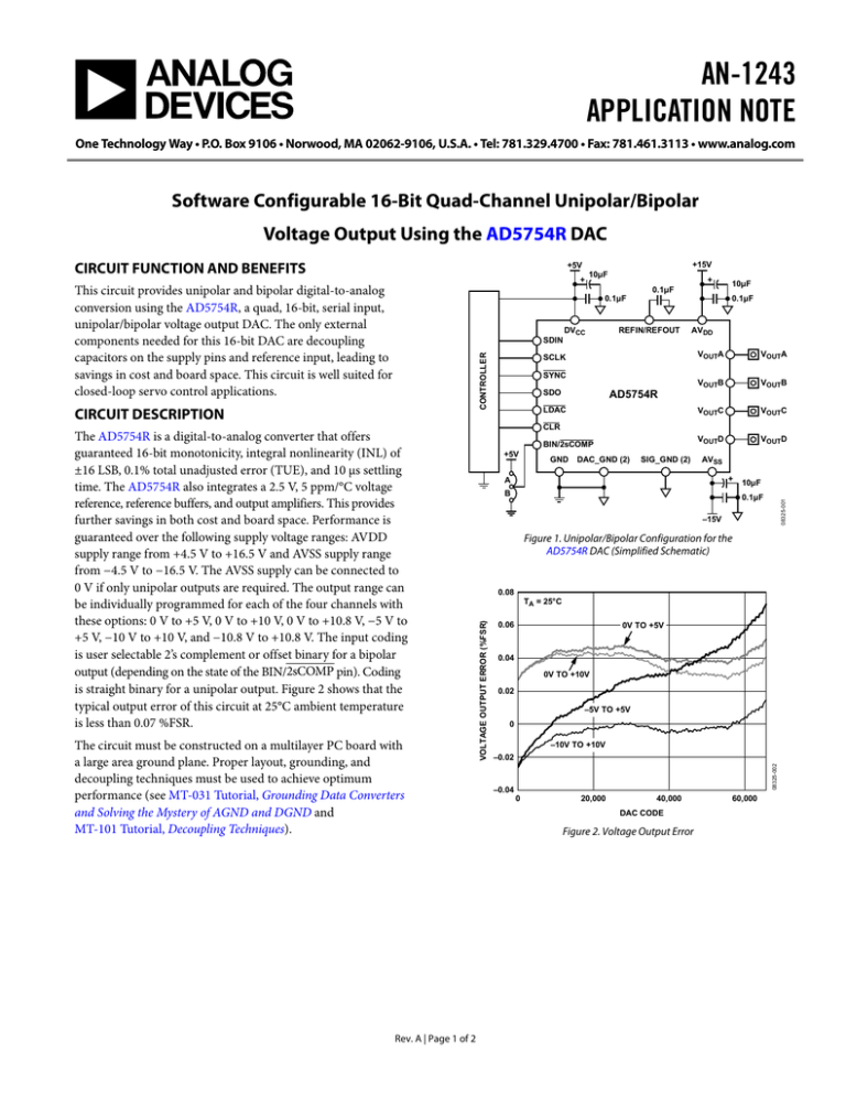
AN-1243 APPLICATION NOTE One Technology Way • P.O. Box 9106 • Norwood, MA 02062-9106, U.S.A. • Tel: 781.329.4700 • Fax: 781.461.3113 • www.analog.com Software Configurable 16-Bit Quad-Channel Unipolar/Bipolar Voltage Output Using the AD5754R DAC +15V + +5V This circuit provides unipolar and bipolar digital-to-analog conversion using the AD5754R, a quad, 16-bit, serial input, unipolar/bipolar voltage output DAC. The only external components needed for this 16-bit DAC are decoupling capacitors on the supply pins and reference input, leading to savings in cost and board space. This circuit is well suited for closed-loop servo control applications. 10μF + CIRCUIT FUNCTION AND BENEFITS 0.1μF DVCC 0.1μF REFIN/REFOUT 10μF 0.1μF AVDD CONTROLLER SDIN Rev. A | Page 1 of 2 VOUTB VOUTB VOUTC VOUTC VOUTD VOUTD AD5754R LDAC BIN/2sCOMP +5V GND DAC_GND (2) SIG_GND (2) AVSS A B 10μF 08325-001 0.1μF –15V Figure 1. Unipolar/Bipolar Configuration for the AD5754R DAC (Simplified Schematic) 0.08 TA = 25°C 0.06 0V TO +5V 0.04 0V TO +10V 0.02 –5V TO +5V 0 –10V TO +10V –0.02 08325-002 The circuit must be constructed on a multilayer PC board with a large area ground plane. Proper layout, grounding, and decoupling techniques must be used to achieve optimum performance (see MT-031 Tutorial, Grounding Data Converters and Solving the Mystery of AGND and DGND and MT-101 Tutorial, Decoupling Techniques). SDO VOUTA + The AD5754R is a digital-to-analog converter that offers guaranteed 16-bit monotonicity, integral nonlinearity (INL) of ±16 LSB, 0.1% total unadjusted error (TUE), and 10 μs settling time. The AD5754R also integrates a 2.5 V, 5 ppm/°C voltage reference, reference buffers, and output amplifiers. This provides further savings in both cost and board space. Performance is guaranteed over the following supply voltage ranges: AVDD supply range from +4.5 V to +16.5 V and AVSS supply range from −4.5 V to −16.5 V. The AVSS supply can be connected to 0 V if only unipolar outputs are required. The output range can be individually programmed for each of the four channels with these options: 0 V to +5 V, 0 V to +10 V, 0 V to +10.8 V, −5 V to +5 V, −10 V to +10 V, and −10.8 V to +10.8 V. The input coding is user selectable 2’s complement or offset binary for a bipolar output (depending on the state of the BIN/2sCOMP pin). Coding is straight binary for a unipolar output. Figure 2 shows that the typical output error of this circuit at 25°C ambient temperature is less than 0.07 %FSR. SYNC VOUTA CLR VOLTAGE OUTPUT ERROR (%FSR) CIRCUIT DESCRIPTION SCLK –0.04 0 20,000 40,000 DAC CODE Figure 2. Voltage Output Error 60,000 AN-1243 Application Note LEARN MORE Data Sheets and Evaluation Boards Kester, Walt. 2005. The Data Conversion Handbook. Analog Devices. Chapters 3 and 7. AD5754R Data Sheet. AD5754R Evaluation Board. MT-015 Tutorial, Basic DAC Architectures II: Binary DACs. Analog Devices. REVISION HISTORY MT-031 Tutorial, Grounding Data Converters and Solving the Mystery of AGND and DGND. Analog Devices. 4/13—Rev. 0 to Rev. A MT-101 Tutorial, Decoupling Techniques. Analog Devices. Changed Document Title from CN-0083 to AN-1243 .............................................................................. Universal Voltage Reference Wizard Design Tool. 7/09—Revision 0: Initial Version ©2009–2013 Analog Devices, Inc. All rights reserved. Trademarks and registered trademarks are the property of their respective owners. AN08325-0-4/13(A) Rev. A | Page 2 of 2
