Evaluation Board for 32-Channel, 14-Bit,
Serial Input, High Voltage Output DACs
EVAL-AD5535EB
FEATURES
AD5535 EVALUATION BOARD POWER SUPPLIES
Full-featured evaluation board
On-board reference
Link options
Direct hook-up to printer port of PC
PC software for control of DACs
The following external supplies must be provided:
•
5 V between the DVCC and DGND inputs for the digital
supply of the AD5535.
•
5 V between the AVCC and AGND inputs for the analog
supply of the AD5535.
•
−5 V between the V− and AGND inputs for the analog
supply of the AD5535.
•
+5 V between the V+ and AGND inputs for the analog
supply of the AD5535.
•
210 V between the VPP and AGND inputs for the analog
supply of the AD5535.
INTRODUCTION
This evaluation board is for the AD5535, 32-channel, 14-bit
high voltage output DAC. The AD5535 contains 32 14-bit
DACs in one package. They have a maximum output voltage
span of 200 V derived from a reference voltage of 4.096 V.
The AD5535 has a serial SPI interface that is compatible with
SPI®, QSPI™, MICROWIRE™, and DSP interface standards.
The DAC outputs are updated on reception of new data into the
DAC registers.
Both AGND and DGND inputs are provided on the board. The
AGND and DGND planes are connected at one location close
to the AD5535. It is recommended not to connect AGND and
DGND elsewhere in the system to avoid ground loop problems.
See the AD5535 data sheet for product details.
Each supply is decoupled to the relevant ground plane with
10 μF and 0.1 μF capacitors. Each device supply pin is again
decoupled with a 10 μF and 0.1 μF capacitor pair to the relevant
ground plane.
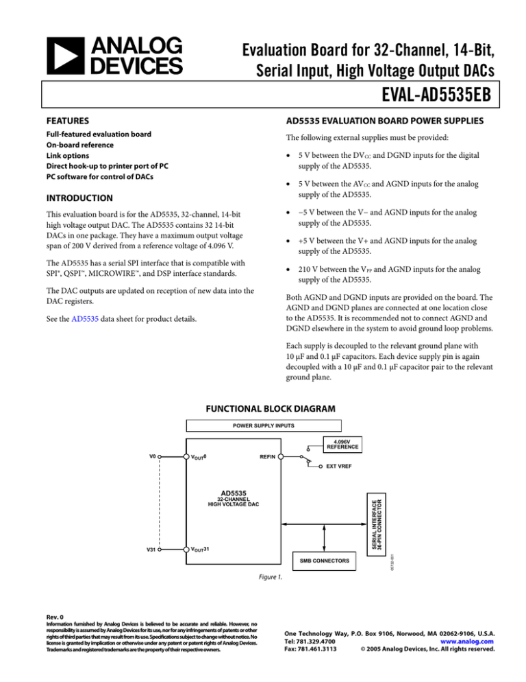
FUNCTIONAL BLOCK DIAGRAM
POWER SUPPLY INPUTS
4.096V
REFERENCE
V0
VOUT0
REFIN
EXT VREF
AD5535
VOUT31
SMB CONNECTORS
05732-001
V31
SERIAL INTERFACE
36-PIN CONNECTOR
32-CHANNEL
HIGH VOLTAGE DAC
Figure 1.
Rev. 0
Information furnished by Analog Devices is believed to be accurate and reliable. However, no
responsibility is assumed by Analog Devices for its use, nor for any infringements of patents or other
rights of third parties that may result from its use. Specifications subject to change without notice. No
license is granted by implication or otherwise under any patent or patent rights of Analog Devices.
Trademarks and registered trademarks are the property of their respective owners.
One Technology Way, P.O. Box 9106, Norwood, MA 02062-9106, U.S.A.
Tel: 781.329.4700
www.analog.com
Fax: 781.461.3113
© 2005 Analog Devices, Inc. All rights reserved.
EVAL-AD5535EB
TABLE OF CONTENTS
Features .............................................................................................. 1
Evaluation Board Software...............................................................4
Introduction ...................................................................................... 1
Software Installation .....................................................................4
AD5535 Evaluation Board Power Supplies ................................... 1
Software Operation .......................................................................4
Functional Block Diagram .............................................................. 1
Component Listing ...........................................................................5
Revision History ............................................................................... 2
ESD Caution...................................................................................5
Link Options ..................................................................................... 3
Evaluation Board Schematics...........................................................6
Default Link Options Setup ........................................................ 3
Ordering Guide .......................................................................... 10
REVISION HISTORY
10/05—Revision 0: Initial Version
Rev. 0 | Page 2 of 12
EVAL-AD5535EB
LINK OPTIONS
The link options on the evaluation board should be set for the required operating setup before using the board. The functions of the link
options are described in Table 1.
Table 1. Link Options
Link No.
LK1
LK2
LK3
LK4
Function
This link selects the voltage reference source for the AD5535:
•
Position A selects an external source via J3 as the voltage reference.
•
Position B selects the on-board 4.096 V reference as the voltage reference source, resulting in a full-scale output
value of 200 V.
•
Position C selects a divided down value of the on-board reference as the voltage reference source (See LK2).
This link selects one of three divided down voltage reference values:
•
Position A selects a value of 3.072 V, resulting in a full-scale output value of 154 V.
•
Position B selects a value of 2.048 V, resulting in a full-scale output value of 102 V.
•
Position C selects a value of 1.024 V, resulting in a full-scale output value of 51 V.
This link selects the state of the TEST pin:
•
In the on position, TEST is connected to DGND, and therefore all DACs are updated on loading of any one DAC.
•
In the off position, TEST is connected to DVCC, and therefore only the addressed DAC is updated.
This link connects the two 5 V (V+ and AVCC) input connectors together:
•
In the on position, the two connectors are connected together and only one requires a power supply connection.
•
In the off position, the two connectors are not connected together and require individual power supply connections.
DEFAULT LINK OPTIONS SETUP
Table 2. Default Link Options
Link No.
LK1
LK2
LK3
LK4
Option
B
B
Off
On
Rev. 0 | Page 3 of 12
EVAL-AD5535EB
EVALUATION BOARD SOFTWARE
SOFTWARE INSTALLATION
The AD5535EB evaluation kit includes self-installing software
on CD-ROM. If the set-up file does not run automatically, you
can run setup.exe from the CD-ROM.
Also, selecting a channel automatically updates that channel
with the value already entered.
To output a squarewave on a DAC channel
The evaluation board software is compatible with Microsoft®
Windows® 95 or better. Ensure that the Centronics cable
connects the PC to the AD5535 evaluation board.
1.
On the Analog Devices menu, click AD5535 Evaluation
Software.
Select Output Squarewave from the Output
Waveform drop-down menu.
2.
A new dialog box opens, as shown in Figure 3.
3.
Type the desired values, pressing ENTER after each
entry.
4.
Click Output Waveform to output the squarewave.
5.
Press any key to stop the waveform output.
05732-003
05732-002
The AD5535 Evaluation Software dialog box is displayed.
Figure 2 shows this box.
1.
Figure 2.
Figure 3.
SOFTWARE OPERATION
The software automatically selects the parallel printer port
address in use by the host PC. Alternative port addresses can be
selected from the Printer Port drop-down menu; the selected
port address is indicated with a check mark.
To load a single code to a DAC channel
1.
Select the desired channel.
2.
Type the desired hexadecimal word.
3.
Press ENTER.
4.
Click on Load All Channels to load all of the 32 DAC
channels with the entered hexadecimal value.
Rev. 0 | Page 4 of 12
EVAL-AD5535EB
COMPONENT LISTING
Table 3.
Qty
1
1
1
4
1
13
11
2
5
2
1
1
1
1
1
9
2
3
1
1
2
2
40
Reference Designator
U1
U2
U3
R1 to R4
R5
C8 to C12, C14 to C17, C19, C26, C31, C33
C1 to C6, C20 to C23, C25
C7, C24
C27 to C30, C38
C13, C18
C32
D1
D2
J1
J2
J3 to J7, J11 to J13, J18
J16, J17
J9, J14, J15
J8
J10
LK1, LK2
LK3, LK4
TP1 to TP7, TP40, V0 to V31
Description
AD5535
REF198AR
AD711KN
1 kΩ, 0.1 W 1% resistor (0805 package)
4k7, 0.1 W 1% resistor (0805 package)
0.1 μF multilayer ceramic capacitor (0603 package)
10 μF tantalum capacitor (TAJ-B package)
10 μF electrolytic 450 V
470 pF, 100 V NPO capacitor (0805 package)
0.01 μF, 1000 V
1μF 35 V tantalum capacitor (TAJ-B package)
SD103C Schottky diode (DO-35 case)
RS1G
36-lead Centronics connector (IEEE 488 style)
40 way 0.1” header (2 × 20)
Gold 50 Ω SMB jack
Black banana socket
Red banana socket
Blue banana socket
Green banana socket
3 way 0.1” header (3 × 1)
2 way 0.1” header (2 × 1)
Test point
ESD CAUTION
ESD (electrostatic discharge) sensitive device. Electrostatic charges as high as 4000 V readily accumulate on
the human body and test equipment and can discharge without detection. Although this product features
proprietary ESD protection circuitry, permanent damage may occur on devices subjected to high energy
electrostatic discharges. Therefore, proper ESD precautions are recommended to avoid performance
degradation or loss of functionality.
Rev. 0 | Page 5 of 12
Supplier/Number
Analog Devices
Analog Devices
Analog Devices
FEC 911-859
FEC 911-938
FEC 499-687
FEC 498-660
FEC 322-8010
FEC 499-195
FEC 219-496
FEC 498-920
Digikey SD103CCT-ND
FEC 547-062
FEC 147-753
FEC 148-535
FEC 310-682
FEC 150-040
FEC 150-039
FEC 150-042
FEC 150-041
FEC 511-717
FEC 511-705
FEC 240-345
C1
10µF
+
2
05732-004
C20
10µF
+
DVCC
J1–5
J1–4
J1–3
J1–2
J1–6
VOUT
100nF
C16
+
C17
100nF
LK3
10µF
V–
U3
OP
6
C28
4
C27
TP3
C29
TP4
100nF
+
10µF
C9
C3
C33
100nF
C30
TP5
C18
100nF
C24 10µF
+
VPP
J1–30
J1–29
J1–28
J1–27
J1–26
J1–25
J1–24
J1–23
J1–22
J1–21
J1–20
J1–19
P7
P10
P9
P8
P4
P2
J16
DGND
TP40
470pF 470pF 470pF 470pF 470pF
C38
TP2
C
LK2
B
A
3
+
V–
DIP-8 PACKAGE
OP196
V+
TP1
2
7
–
C
B
AVCC
DVCC
R5
4kΩ
C23
TEST
J18
100nF
C22 10µF
+
V+
SYNCB
R1
1kΩ
R4
1kΩ
R2
1kΩ
R3
1kΩ
CLOSE TO POWER SOCKETS
C21 10µF
C15
AVCC
SDIN
J12
100nF +
C14
SCLK
J11
1µF
+ C32
J13
100nF
C31
6
10µF DECOUPLING
FOR U3
C26
C25
4
GND
REF198
100nF
+
VIN
SO-8 PACKAGE
U2
AVCC
100nF
C19
AVCC
CENTRONICS
J14
TEST
SYNCB
SCLK
DIN
RESETB
REFIN
LK4
V+
V–
J10
J9
V+
+5V
+
C5
10µF
U1
AD5535
D2
J8
VPP
+275V
VPP
100nF
AVCC C11
V–
–5V
DVCC AVCC
J15
DVCC AVCC
+5V
+5V
+
C4
10µF
100nF
DVCC C10
DVCC
LK1
A
M13
AVCC2 M14
AVCC1
J3
K1
V+1
V + 2 K2
CATHODE
RS1G
+
C13
C7
10µF
J17
J4
VOUT0
VOUT1
VOUT2
VOUT3
VOUT4
VOUT5
VOUT6
VOUT7
VOUT8
VOUT9
VOUT10
VOUT11
VOUT12
VOUT13
VOUT14
VOUT15
VOUT16
VOUT17
VOUT18
VOUT19
VOUT20
VOUT21
VOUT22
VOUT23
VOUT24
VOUT25
VOUT26
VOUT27
VOUT28
VOUT29
VOUT30
VOUT31
VOUT30
B1
A2
D1
C2
B3
E2
F3
A4
E4
B5
F5
A6
E6
B7
F7
E8
A8
B9
F9
E10
A10
B11
C12
D13
E12
A12
B13
H13
G14
C14
F13
E14
C36
R8
D1
V–
C37
R9
C34
R6
J5
VOUT31
J6
VOUT0
CLOSE TO U1
SD103C
+
C6
10µF
C12
+
C2
10µF
V+
100nF
C8
100nF
AGND
V–
100nF
H1
VPP1
VPP2 H2
ANODE
P5
DGND
P6
L2
V–2
V – 1 L1
M2
AGND2
M1
AGND1
P3
DACGND1
L14
DACGND2
N1
PGND1
N2
PGND2
Rev. 0 | Page 6 of 12
N3
Figure 4. Evaluation Board Circuit Diagram
N4
EXT VREF
C35
R7
J7
VOUT1
TP6
TP7
V0
V1
V2
V3
V4
V5
V6
V7
V8
V9
V10
V11
V12
V13
V14
V15
V16
V17
V18
V19
V20
V21
V22
V23
V24
V25
V26
V27
V28
V29
V30
V31
J2–4
J2–3
J2–10
J2–11
J2–7
J2–9
J2–12
J2–6
J2–5
J2–14
J2–13
J2–15
J2–8
J2–17
J2–16
J2–18
J2–22
J2–19
J2–20
J2–21
J2–33
J2–25
J2–23
J2–24
J2–27
J2–30
J2–31
J2–26
J2–28
J2–36
J2–35
J2–29
J2–34
J2–32
J2–38
J2–39
J2–40
J2–37
J2–2
J2–1
EVAL-AD5535EB
EVALUATION BOARD SCHEMATICS
PIN HEADER
05732-005
EVAL-AD5535EB
Figure 5. Component Side PCB Layout Diagram
Rev. 0 | Page 7 of 12
05732-006
EVAL-AD5535EB
Figure 6. Solder Side PCB Layout Diagram
Rev. 0 | Page 8 of 12
05732-007
EVAL-AD5535EB
Figure 7. Component Placement Diagram
Rev. 0 | Page 9 of 12
EVAL-AD5535EB
ORDERING GUIDE
Model
EVAL-AD5535EB
Description
AD5535 Evaluation Board Kit
Rev. 0 | Page 10 of 12
EVAL-AD5535EB
NOTES
Rev. 0 | Page 11 of 12
EVAL-AD5535EB
NOTES
© 2005 Analog Devices, Inc. All rights reserved. Trademarks and
registered trademarks are the property of their respective owners.
EB05732–0–10/05(0)
Rev. 0 | Page 12 of 12
