Section 6. Interfacing to the DDS Output
advertisement
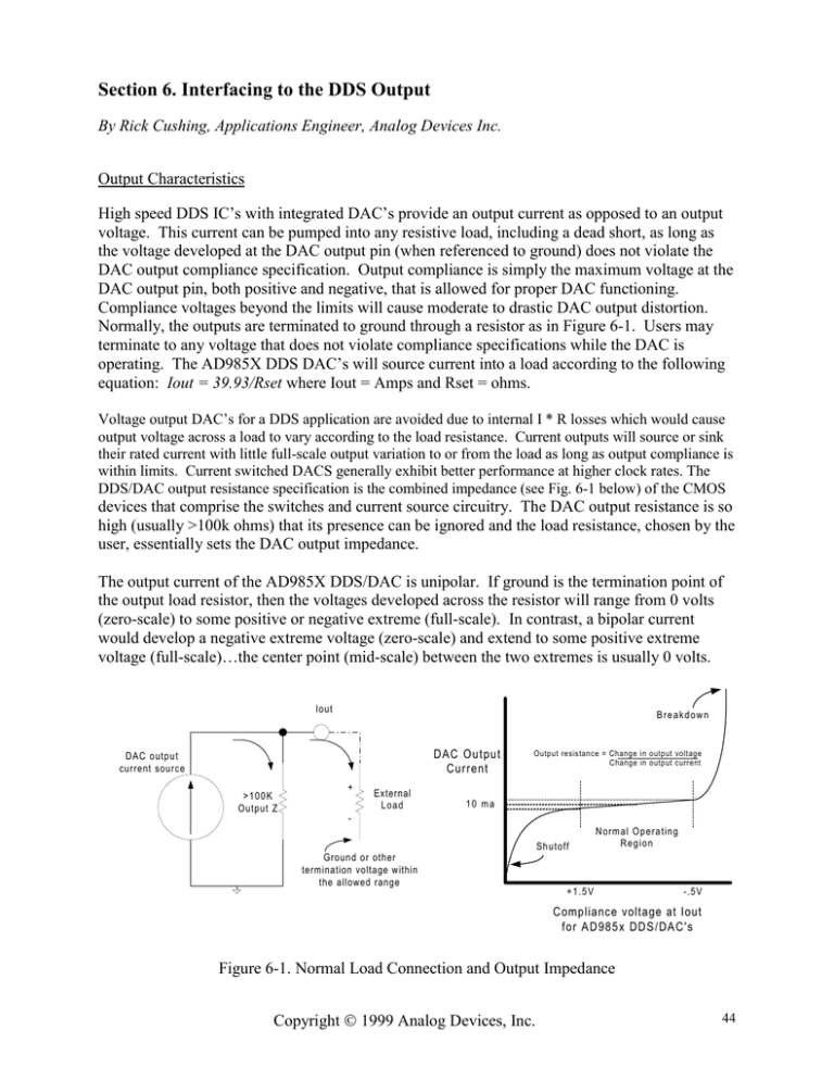
Section 6. Interfacing to the DDS Output By Rick Cushing, Applications Engineer, Analog Devices Inc. Output Characteristics High speed DDS IC’s with integrated DAC’s provide an output current as opposed to an output voltage. This current can be pumped into any resistive load, including a dead short, as long as the voltage developed at the DAC output pin (when referenced to ground) does not violate the DAC output compliance specification. Output compliance is simply the maximum voltage at the DAC output pin, both positive and negative, that is allowed for proper DAC functioning. Compliance voltages beyond the limits will cause moderate to drastic DAC output distortion. Normally, the outputs are terminated to ground through a resistor as in Figure 6-1. Users may terminate to any voltage that does not violate compliance specifications while the DAC is operating. The AD985X DDS DAC’s will source current into a load according to the following equation: Iout = 39.93/Rset where Iout = Amps and Rset = ohms. Voltage output DAC’s for a DDS application are avoided due to internal I * R losses which would cause output voltage across a load to vary according to the load resistance. Current outputs will source or sink their rated current with little full-scale output variation to or from the load as long as output compliance is within limits. Current switched DACS generally exhibit better performance at higher clock rates. The DDS/DAC output resistance specification is the combined impedance (see Fig. 6-1 below) of the CMOS devices that comprise the switches and current source circuitry. The DAC output resistance is so high (usually >100k ohms) that its presence can be ignored and the load resistance, chosen by the user, essentially sets the DAC output impedance. The output current of the AD985X DDS/DAC is unipolar. If ground is the termination point of the output load resistor, then the voltages developed across the resistor will range from 0 volts (zero-scale) to some positive or negative extreme (full-scale). In contrast, a bipolar current would develop a negative extreme voltage (zero-scale) and extend to some positive extreme voltage (full-scale)…the center point (mid-scale) between the two extremes is usually 0 volts. Iout Breakdown DAC Output Current DAC output current source >100K Output Z + External Load Output resistance = Change in output voltage Change in output current 10 ma Shutoff Normal Operating Region Ground or other termination voltage within the allowed range +1.5V -.5V Compliance voltage at Iout for AD985x DDS/DAC's Figure 6-1. Normal Load Connection and Output Impedance Copyright 1999 Analog Devices, Inc. 44 Why does unipolar current matter? First, the center point of the DDS output sine wave will be dc-offset from the load termination potential by one-half of the full-scale voltage. This may be an important consideration when applying this signal to a dc coupled amplifier since the dc component could cause amplifier clipping. Second, when AM modulating the output power envelope using the Rset resistor, the modulation envelope will be asymmetrical, looking more like a pulsed output (Figure 6-2B) than a symmetrically modulated carrier (Figure 6-2A). For more information regarding AM modulation of a DDS see Analog Devices application note AN423, available on the Analog Devices website. Figure 6-2. A-Symmetrical AM Modulated RF Envelope; B- Asymmetrical AM Modulation Produced from a Unipolar Current Output by Modulating the Rset Resistor Copyright 1999 Analog Devices, Inc. 45 Transformer vs Single-ended Output Coupling The DDS DAC output of the AD985X series is actually composed of two outputs, 180 degrees out of phase with each other (the true and complement). These two signals can be combined in a center-tapped RF transformer to produce the symmetrical waveform seen in Figure 6-2A. In the beginning of this section the equation for Iout was given. This equation actually defines the sum Figure 6-3. Combining Complementary Outputs to Achieve Symmetrical Output Envelope Copyright 1999 Analog Devices, Inc. 46 of the two currents available from the Iout and IoutB outputs. For example, if Rset is set for10 ma full-scale, then if one output is at 2 ma, the other must be at 8 ma…if one is at 0 ma, the other must be at 10 ma, etc. By combining these two complementary currents in a transformer as in Figure 6-3, the output envelope becomes symmetrical and the dc offset is lost. Transformer coupling is also beneficial in coupling the DAC current-outputs to reactive inputs, such as LC filters (Figure 6-4A). The low impedance pathway to ground through the transformer center tap is far better than taking the reactive pathway through an LC filter that is terminated only at the filter output (Figure 6-4C). Without a transformer, the next best method is to apply the DAC current output to a LC filter that is doubly-terminated, as shown in Figure 6-4B. The arrows in Figure 6-3 show current flow in the broadband 1:1 transformer primary and how the unipolar current of two complementary outputs can be used to simulate a bipolar current. The 50-ohm load resistance at the transformer secondary is reflected to the transformer center-tapped primary where it looks like a 25-ohm load for each output. Different turns-ratios will allow different loads to be used without violating the DDS DAC output compliance specification. The voltages developed at pins 20 and 21 (of an AD985X DDS) in Figures 6-3 and 6-4A will no longer be unipolar as they would be if each pin were driving a resistive load to ground (Figure 64B & C). Instead, the voltages will be bipolar and symmetrical around the voltage present at the center-tap - ground in this instance. This transformation from unipolar to bipolar voltage is to be expected as the magnetic fields of the center-tapped primary build and collapse. Users should pay attention to the negative compliance voltage as well as the positive compliance voltage when configuring the outputs for transformer coupling. 21 20 LC Filter Iout IoutB A 21 20 LC Filter Iout IoutB B 21 20 LC Filter Iout IoutB C Figure 6-4: Coupling Reactive Loads to the DDS DAC Output Copyright 1999 Analog Devices, Inc. 47 Another benefit to transformer coupling is the phenomenon of common mode rejection. If the DDS DAC outputs (Iout and IoutB) contain signals that are common or identical to each other…such as clock feedthrough, ac power supply components, or other spurious signals, then these signals can be reduced or eliminated from the output spectrum by transformer coupling. If identical signals are presented to the two transformer primary inputs as in Figure 6-4A, then their opposing fields will cancel each other to some degree. The degree of cancellation is dependent upon the transformer winding matching as well as the matching of the two “identical “ signals Output Power Considerations Combining the two complementary outputs in a transformer does not offer any power gain. In the AD985X series of DDS IC’s, the only way to increase output power is to set the output current to a higher value by adjusting Rset. Up to 20 ma maximum output current is commonly available; however, harmonic distortion of the output may also increase slightly. Use of a transformer (Figure 6-4A) does permit more efficient transfer of power to a load by eliminating the need for an input termination resistor (Figure 6-4B) which dissipates power that should have been transferred to the output termination resistor. Output power into a 50-Ohm load for a 20 ma full-scale output sine wave is 2.5 mW or +4 dBm. Output power into the same load for a 10 ma full-scale output sine wave is .625 mW or -2 dBm. Output power is determined using the equation P = E2/R, where E is the RMS voltage developed across the load resistance, R. P, of course, is measured in Watts. The units of dBm are arrived at using 10 * LOG (P) where P is expressed in milliWatts. As a reminder, the term dBm expresses an absolute relationship between the power level of one milliWatt and some other power level. The term dB expresses the power level of some arbitrary reference to another power level and therefore, it is a relative measurement. DDS/DAC Output Termination Regardless of what output termination scheme is chosen, experience has shown that optimum spurious and harmonic suppression are achieved when both Iout and IoutB outputs are terminated equally. Failure to do so may not be noticed at lower frequencies, but at higher output frequencies, where every dB of SFDR (spurious-free dynamic range) counts, this practice will give a cleaner output spectrum, lower spurs and higher SFDR. This practice is especially applicable to situations where only one of the outputs is utilized. Copyright 1999 Analog Devices, Inc. 48
