AN-831 APPLICATION NOTE
advertisement

AN-831
APPLICATION NOTE
One Technology Way • P.O. Box 9106 • Norwood, MA 02062-9106, U.S.A. • Tel: 781.329.4700 • Fax: 781.461.3113 • www.analog.com
Implementing a Counter with the ADuC702x Family
by Aude Richard
Table 1. Transition Table
INTRODUCTION
The ADuC702x family has an on-chip programmable logic
array that consists of 16 gates with flip-flops on the output. This
glue logic can be used for different functions. This application
note describes how to implement a 3-bit counter but it can also
apply to a simple sequence generation.
THE PLA
The programmable logic array (PLA) can be described as glue
logic and its function is to remove the requirement for simple
external logic. It consists of two independent blocks of eight
elements. The two blocks can have different clocks, however,
each element within a block uses the same block clock.
Each of the 16 elements contains a two-input look-up table and
a flip-flop. The look-up table can be configured to generate any
logic function based on one or two inputs. The flip-flop can be
clocked with the block clock or it can be bypassed.
State
0
1
2
3
4
5
6
7
Actual Outputs
Q1
Q0
0
0
0
1
1
0
1
1
0
0
0
1
1
0
1
1
Q2
0
0
0
0
1
1
1
1
Next Outputs
D1
D0
0
1
1
0
1
1
0
0
0
1
1
0
1
1
0
0
D2
0
0
0
1
1
1
1
0
Table 2. Functions
D2
Q2
00
0
1
0
1
01
0
1
Q1, Q0
11
1
0
10
0
1
01
1
1
Q1, Q0
11
0
0
10
1
1
D2 = Q2Q1Q0 + Q2Q1 + Q2Q0
0
4
2
3
A
B
D1
Q2
LOOK-UP
TABLE
1
00
0
0
0
1
05852-001
D1 = Q1Q0 + Q1 Q0 = Q1 ⊕ Q0
D0 = Q0
Figure 1. PLA Element
SYNCHRONOUS COUNTER
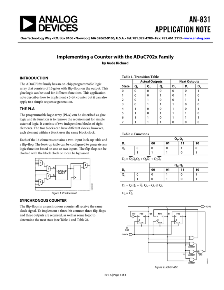
The flip-flops in a synchronous counter all receive the same
clock signal. To implement a three-bit counter, three flip-flops
and three outputs are required, as well as some logic to
determine the next state (see Table 1 and Table 2).
Q[2:0]
FDC
INV
D
C
CLR
FDC
Q0
Q
D
C
CLR
FDC
Q1
Q
D
Q
C
CLR
GND
CLOCK
AND3B1
AND2B1
AND2B1
Figure 2. Schematic
Rev. A | Page 1 of 4
OR3
05852-002
Q2
AN-831
Application Note
IMPLEMENTATION ON THE ADUC702x
CONCLUSION
To implement a three-bit counter, three flip-flops and three
general-purpose outputs are required.
There are three main advantages to implementing a 3-bit
counter using the PLA:
Because each PLA element contains only a two input gate, the
three input gates need to be replaced with two input gates.
•
There is no requirement for an external component.
•
As an integrated solution, no processing power is required.
•
The clock is fully programmable, with no requirement for
an external clock signal.
D2 can also be written as
D2 = Q2Q1Q0 + Q2Q1 + Q2Q0 = Q2Q1Q0 + Q2Q1Q0
This can easily be implemented with two input gates.
Note that the clock used for the flip-flops is fully
programmable. It can be one of three GPIOs: the HCLK,
internal oscillator, or Timer 1 overflow. The Timer 1 overflow
offers a great deal of flexibility with four clock sources, a
prescaler, and a 32-bit counter.
Q0
This application note only discusses the case of a 3-bit counter.
However, any simple sequence generation can be easily implemented using the same technique.
The main disadvantage of this technique is due to the limited
number of gates and outputs available on the part.
The graphical PLA configuration tool is available to download
on Analog Devices’ website, www.analog.com.
ELEMENT 7
CLK
Q1
ELEMENT 6
ELEMENT 1
CLK
Q0
Q2
ELEMENT 2
Q1
ELEMENT 0
ELEMENT 5
ELEMENT 3
CLK
05852-003
Q2
Figure 3. Implementation Using the PLA Tool
Rev. A | Page 2 of 4
Application Note
AN-831
Table 3. Relevant Extract from Companion Code PLAinit.c
//Code Generated By the ADuC 702X PLA Tool
//FileType:
C PLA Configuration File
//Source:
C Source Code
//Date:
24/10/2005 22:20:13
//================================================================
#include "ADuC7026.h"
void
plaInitialize( )
{
// Configure Port Pins for PLA mode
//
In order for the PLA Tool to configure the required GPIO pins
//
you must make the necessary selections on the outputs tab!!!
GP1CON = 0x30000000;
GP2CON = 0x00000330;
// Configure individual elements
PLAELM0 = 0x02DC;
PLAELM1 = 0x07CF;
PLAELM2 = 0x0051;
PLAELM3 = 0x0145;
PLAELM5 = 0x07D1;
PLAELM6 = 0x07CC;
PLAELM7 = 0x018A;
// Clk Source configuration
PLACLK = 0x0004;
}
Rev. A | Page 3 of 4
AN-831
Application Note
NOTES
©2011 Analog Devices, Inc. All rights reserved. Trademarks and
registered trademarks are the property of their respective owners.
AN05852-0-1/11(A)
Rev. A | Page 4 of 4


