AN-1078 APPLICATION NOTE
advertisement
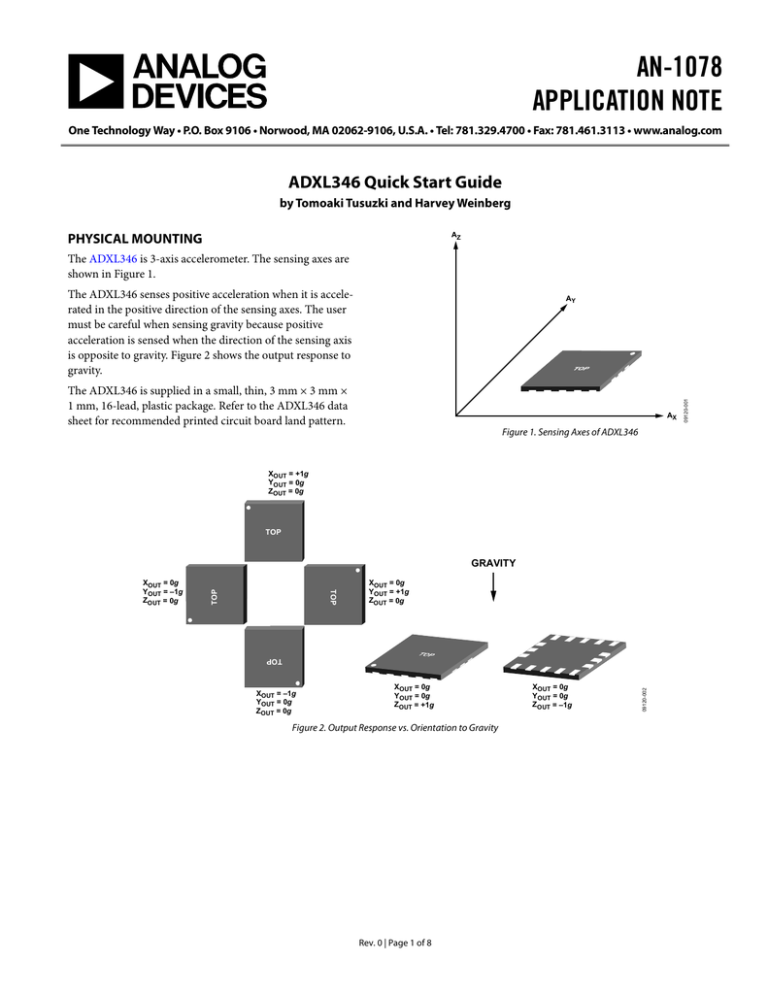
AN-1078 APPLICATION NOTE One Technology Way • P.O. Box 9106 • Norwood, MA 02062-9106, U.S.A. • Tel: 781.329.4700 • Fax: 781.461.3113 • www.analog.com ADXL346 Quick Start Guide by Tomoaki Tusuzki and Harvey Weinberg AZ PHYSICAL MOUNTING The ADXL346 is 3-axis accelerometer. The sensing axes are shown in Figure 1. The ADXL346 senses positive acceleration when it is accelerated in the positive direction of the sensing axes. The user must be careful when sensing gravity because positive acceleration is sensed when the direction of the sensing axis is opposite to gravity. Figure 2 shows the output response to gravity. The ADXL346 is supplied in a small, thin, 3 mm × 3 mm × 1 mm, 16-lead, plastic package. Refer to the ADXL346 data sheet for recommended printed circuit board land pattern. AX Figure 1. Sensing Axes of ADXL346 XOUT = +1g YOUT = 0g ZOUT = 0g TOP TOP XOUT = 0g YOUT = +1g ZOUT = 0g XOUT = –1g YOUT = 0g ZOUT = 0g XOUT = 0g YOUT = 0g ZOUT = +1g Figure 2. Output Response vs. Orientation to Gravity Rev. 0 | Page 1 of 8 XOUT = 0g YOUT = 0g ZOUT = –1g 09120-002 TOP XOUT = 0g YOUT = –1g ZOUT = 0g TOP GRAVITY 09120-001 AY AN-1078 Application Note TABLE OF CONTENTS Physical Mounting ............................................................................ 1 Reading Output Data ....................................................................4 Electrical Connection .................................................................. 3 Data Format ...................................................................................4 Communication Interface ........................................................... 3 Using Self-Test ...............................................................................5 Initialization .................................................................................. 3 Using Offset Registers ...................................................................6 Rev. 0 | Page 2 of 8 Application Note AN-1078 ELECTRICAL CONNECTION COMMUNICATION INTERFACE 2 ADXL346 communication is done via either I C or SPI (3- or 4-wire). Figure 3 shows the recommended electrical connections for 4-wire SPI mode. Note that the SDO pin can be disconnected when using 3-wire SPI mode. VS Table 1 gives the list of typical configuration settings for the master processor requirements for SPI communication with the ADXL346. These settings are normally in control registers. Refer to the ADXL346 data sheet for timing specification and command sequence. VDD I/O CS Table 1. SPI Settings CIO Processor Setting Master SPI Mode VDD I/O ADXL346 PROCESSOR CS D OUT SDA/SDI/SDIO D OUT SCL/SCLK D OUT SDO/ALT ADDRESS D IN INT1 D IN INT2 D IN Bit Sequence Description ADXL346 operates as slave Clock polarity (CPOL) = 1 Clock phase (CPHA) = 1 MSB first mode For I2C communication, refer to the ADXL346 data sheet and UM10204 I2C-Bus Specification and User Manual, Rev. 03—19 June 2007 for processor settings as well as timing specifications and command sequence. 09120-003 VS Figure 3. Recommended Connection for 4-Wire SPI Mode Figure 4 shows the recommended electrical connection for I2C mode. The 7-bit I2C address for the device is 0x53, followed by the R/W bit. The user can select alternate I2C address by connecting an SDO/ALT ADDRESS pin to the VDD I/O pin. The 7-bit I2C address for that configuration is 0x1D, followed by the R/W bit. VDD I/O Sometimes it is important to confirm the validity of communication before going to the next design stage. This can be done by reading the DEVID register (Address 0x00). It is a read only register that contains 0xE6. If the data read from DEVID is not 0xE6, it is the indication that either the physical connection or command sequence is incorrect. INITIALIZATION RP RP PROCESSOR Figure 5 shows the minimum initialization sequence. The ADXL346 operates in a 100 Hz ODR with the DATA_READY interrupt on the INT1 pin during this start-up sequence. When setting other interrupts or using the FIFO, it is recommended that those registers used are set before the POWER_CTL and INT_ENABLE registers. Refer to the ADXL346 data sheet and AN-1025 Application Note for other operation modes of the ADXL346 and details about FIFO. CS D IN/OUT SDA D OUT SCL 09120-004 ALT ADDRESS Figure 4. Recommended Connection for I2C Mode Refer to the ADXL346 data sheet for details on power supply decoupling. START VS = ON VDD I/O = ON WAIT 1.1ms INITIALIZE COMMAND SEQUENCE END STEP REGISTER ADDRESS REGISTER NAME 1 0x31 DATA_FORMAT 0x0B 2 0x2D POWER_CTL 0x08 START MEASUREMENT 3 0x2E INT_ENABLE 0x80 ENABLE DATA_READY INTERRUPT DATA Figure 5. Minimum Initialization Sequence Rev. 0 | Page 3 of 8 DESCRIPTION ±16g, 13-BIT MODE 09120-005 ADXL346 AN-1078 Application Note formats are available by setting the DATA_FORMAT register. See the ADXL346 data sheet for more details. READING OUTPUT DATA The DATA_READY interrupt signal indicates that 3-axis acceleration data is updated in the data registers. It is latched high when new data is ready. (The interrupt can be configured to be latched from low-to-high through the DATA_FORMAT register. Refer to the ADXL346 data sheet for details.) Use the low-to-high transition to trigger action on an interrupt service routine. Data is read from DATAX0, DATAX1, DATAY0, DATAY1, DATAZ0, and DATAZ1 registers. To ensure data coherency, it is recommended that multibyte reads are used to retrieve data from ADXL346. Figure 7 shows the read sequence example for 4-wire SPI. The ADXL346 uses twos complement data format. When in 13-bit mode, 1 LSB represents about 3.9 mg. Table 2. ADXL346 Output Data Format DATA FORMAT The data format of the ADXL346 is 16 bits. Once acceleration data is acquired from data registers, the user must reconstruct the data. DATAX0 is the low byte register for X-axis acceleration and DATAX1 is the high byte register. In 13-bit mode, the upper 4 bits are sign bits (see Figure 6). Note that other data D15 D14 D13 D12 Twos Complement Representation (Dec) 4095 … +2 +1 0 −1 −2 … −4095 D11 D10 D9 D8 D7 D6 D5 D4 D3 D2 D1 D0 SIGN SIGN SIGN SIGN D11 D10 D9 D8 D7 D6 D5 D4 D3 D2 D1 D0 DATAX0 DATAY0 DATAZ0 DATAX1 DATAY1 DATAZ1 Acceleration (mg) +1599 … +7.8 +3.9 0 −3.9 −7.8 … −1600 09120-007 16-Bit Code (Hex) 0FFF … 0002 0001 0000 FFFF FFFE … F000 Figure 6. Data Construction INT1 PIN CS SCLK SDI DATAX1 DATAZ1 09120-006 DATAX0 SDO 0xF2 Figure 7. Data Read Timing Sequence for 4-Wire SPI Connection Rev. 0 | Page 4 of 8 Application Note AN-1078 USING THE SELF-TEST FEATURE The ADXL346 provides a self-test feature that enables an electromechanical test on the device without external mechanical stimulus. Figure 8 outlines a recommended selftest sequence. Note that the ADXL346 should be placed in a stable environment when conducting the self-test sequence. START VS = ON VDD I/O = ON WAIT 1.1ms INITIAL COMMAND SEQUENCE WAIT 1.1ms TAKE 100 DATA POINTS AND AVERAGE ACTIVATE SELF-TEST STEP REGISTER ADDRESS REGISTER NAME DATA 1 0x31 DATA_FORMAT 0x0B ±16g, 13-BIT MODE 2 0x2D POWER_CTL 0x08 START MEASUREMENT 3 0x2E INT_ENABLE 0x80 ENABLE DATA_READY INTERRUPT WHEN AT ODR = 100Hz (WAIT TIME DEPENDS ON ODR SETTLING AND 1.1ms + 1/ODR) IT IS TO MINIMIZE THE EFFECT OF NOISE STEP REGISTER ADDRESS REGISTER NAME DATA DESCRIPTION 1 0x31 DATA_FORMAT 0x8B SELF-TEST ON, ±16g, 13-BIT MODE WAIT 1.1ms TAKE 100 DATA POINTS AND AVERAGE INACTIVATE SELF-TEST DESCRIPTION IT IS TO MINIMIZE THE EFFECT OF NOISE STEP REGISTER ADDRESS REGISTER NAME DATA DESCRIPTION 1 0x31 DATA_FORMAT 0x0B SELF-TEST OFF, ±16g, 13-BIT MODE 09120-008 CALCULATE SELF-TEST DELTA AND COMPARE IT TO DATASHEET LIMITS END Figure 8. Self-Test Sequence Rev. 0 | Page 5 of 8 AN-1078 Application Note register to measured acceleration. For example, if the offset is +156 mg, then −156 mg should be written to offset register. Figure 9 shows the typical offset calibration sequence. USING OFFSET REGISTERS The ADXL346 has offset registers that facilitate offset calibration. The data format for the offset registers is 8-bit, twos compliment. The resolution of the offset registers about 15.6 mg/LSB. If the offset calibration must be finer than 15.6 mg/LSB, the calibration needs to be done at the processor. The offset register adds the value written in the For this routine, X-/Y-axes errors are zero when 0 g input is applied, whereas Z-axis errors are zero when 1 g input is applied. Greater accuracy can be achieved if it is possible to rotate the ADXL346 at calibration. START PLACE SENSOR IN X = 0g, Y = 0g, Z = +1g ORIENTATION VS = ON VDD I/O = ON INITIALIZE COMMAND SEQUENCE WAIT 11.1ms TAKE 100 DATA POINTS AND AVERAGE CALCULATE CALIBRATION VALUE WRITE TO OFSTx REGISTERS END STEP 1 2 3 REGISTER ADDRESS 0x31 0x2D 0x2E REGISTER NAME DATA_FORMAT POWER_CTL INT_ENABLE DATA 0x0B 0x08 0x80 DESCRIPTION ±16g, 13-BIT MODE START MEASUREMENT ENABLE DATA_READY INTERRUPT WHEN AT ODR = 100Hz (WAIT TIME DEPENDS ON ODR SETTLING AND 1.1ms + 1/ODR) IT IS TO MINIMIZE THE EFFECT OF NOISE X_CALIB = –(OUTPUT (X) ÷ 4) Y_CALIB = –(OUTPUT (Y) ÷ 4) Z_CALIB = –((OUTPUT (Z) – 256) ÷ 4) STEP 1 2 3 REGISTER ADDRESS 0x1E 0x1F 0x20 REGISTER NAME OFSTX OFSTY OFSTZ DATA X_CALIB Y_CALIB Z_CALIB Figure 9. Offset Calibration Sequence Rev. 0 | Page 6 of 8 DESCRIPTION X_CALIB TO BE 8 BIT Y_CALIB TO BE 8 BIT Z_CALIB TO BE 8 BIT 09120-009 WAIT 1.1ms Application Note AN-1078 NOTES Rev. 0 | Page 7 of 8 AN-1078 Application Note NOTES ©2010 Analog Devices, Inc. All rights reserved. Trademarks and registered trademarks are the property of their respective owners. AN09120-0-6/10(0) Rev. 0 | Page 8 of 8
