AN-1204 APPLICATION NOTE
advertisement
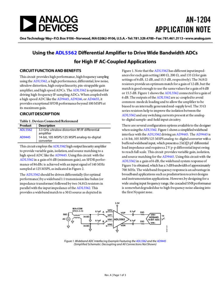
AN-1204 APPLICATION NOTE One Technology Way • P.O. Box 9106 • Norwood, MA 02062-9106, U.S.A. • Tel: 781.329.4700 • Fax: 781.461.3113 • www.analog.com Using the ADL5562 Differential Amplifier to Drive Wide Bandwidth ADCs for High IF AC-Coupled Applications CIRCUIT FUNCTION AND BENEFITS Figure 1. Note that the ADL5562 has different input impedances for each gain setting (400 Ω, 200 Ω, and 133 Ω for gain settings of 6 dB, 12 dB, and 15.5 dB, respectively). The 34.8 Ω resistors provide an optimum match for a gain of 12 dB, but the match is good enough to use the same values for a gain of 6 dB or 15.5 dB. Figure 1 shows the ADL5562 connected for a gain of 6 dB. The outputs of the ADL5562 are ac-coupled to avoid common-mode dc loading and to allow the amplifier to be biased to an internally generated mid-supply level. The 33 Ω series resistors help to improve the isolation between the ADL5562 and any switching currents present at the analogto-digital sample-and-hold input circuitry. This circuit provides high performance, high frequency sampling using the ADL5562, a high performance, differential, low noise, ultralow distortion, high output linearity, pin-strappable gain amplifier, and high speed ADCs. The ADL5562 is optimized for driving high frequency IF sampling ADCs. When coupled with a high speed ADC like the AD9445, AD9246, or AD6655, it provides exceptional SFDR performance beyond 100 MSPS at its maximum gain. CIRCUIT DESCRIPTION Table 1. Devices Connected/Referenced AD9445 There are several configuration options available to the designer when using the ADL5562. Figure 1 shows a simplified wideband interface with the ADL5562 driving an AD9445. The AD9445 is a 14-bit, 105 MSPS/125 MSPS analog-to-digital converter with a buffered wideband input, which presents a 2 kΩ||3 pF differential load impedance and requires a 2 V p-p differential input swing to reach full scale. This circuit provides variable gain, isolation, and source matching for the AD9445. Using this circuit with the ADL5562 in a gain of 6 dB, the wideband system response of Figure 3 is obtained, which has a 3 dB bandwidth of approximately 700 MHz. The wideband frequency response is an advantage in broadband applications such as predistortion receiver designs and instrumentation applications. However, by designing for a wide analog input frequency range, the cascaded SNR performance is somewhat degraded due to high frequency noise aliasing into the first Nyquist zone. Description 3.3 GHz ultralow distortion RF/IF differential amplifier 14-bit, 105 MSPS/125 MSPS analog-to-digital converter This circuit employs the ADL5562 high output linearity amplifier to provide variable gain, isolation, and source matching to a high speed ADC like the AD9445. Using this circuit with the ADL5562 in a gain of 6 dB (minimum gain), an SFDR performance of 84 dBc is achieved with an input signal of 140 MHz sampled at 125 MSPS, as indicated in Figure 2. The ADL5562 should be driven differentially (for optimal performance) by a wideband 1:1 transmission line balun (or impedance transformer) followed by two 34.8 Ω resistors in parallel with the input impedance of the ADL5562. This provides a wideband match to a 50 Ω source as depicted in 3.3V M/A-COM ETC1-1-13 50Ω AC 0.1µF A VOP 0.1µF 33Ω VIP1 34.8Ω 0.1µF B 34.8Ω VIP2 VIN1 ADL5562 VIN2 VIN+ AD9445 0.1µF 33Ω 14 14-BIT ADC VIN– VON Figure 1. Wideband ADC Interfacing Example Featuring the ADL5562 and the AD9445 (Simplified Schematic: Decoupling and All Connections Not Shown) Rev. A | Page 1 of 3 08397-001 Product ADL5562 AN-1204 Application Note 0 0 ADL5562 DRIVING THE AD9445 14-BIT ADC GAIN = 6dB INPUT = 140MHz SAMPLING RATE = 125MSPS SNR = 66.25dBc SFDR = 84.2dBc NOISE FLOOR = –109.5dB FUND = –1.081dBFS SECOND = –84.54dBc THIRD = –84.54dBc –20 –30 –40 –50 –2 –3 –4 –70 –80 –5 –6 –90 –100 –7 –110 FIRST POINT = –1.02dBFS END POINT = –5.69dBFS MID POINT = –1.09dBFS MIN = –5.69dBFS MAX = –0.88dBFS –8 –120 –130 –9 –140 –10 2.00 0 6.25 12.50 18.75 25.00 31.25 37.50 43.75 50.00 56.25 62.50 FREQUENCY (MHz) 08397-002 –150 81.90 Figure 2. Measured Single-Tone Performance of the Circuit in Figure 1 for a 140 MHz Input Signal Sampled at 125 MSPS 641.20 481.40 801.00 321.60 161.80 561.30 721.10 241.70 401.50 FREQUENCY (MHz) Figure 3. Measured Frequency Response of Wideband Circuit in Figure 1 zero into the transfer function. The 1 nF ac coupling capacitors introduce additional zeros into the transfer function. The final overall frequency response takes on a band-pass characteristic, helping to reject noise outside of the intended Nyquist zone. Table 2 provides initial suggestions for prototyping purposes. Some empirical optimization may be needed to help compensate for actual PCB parasitics. Details of designing the interstage filters can be found in application notes AN-827, A Resonant Approach to Interfacing Amplifiers to Switched Capacitor ADCs, and AN-742, Frequency Domain Response of Switched Capacitor ADCs. COMMON VARIATIONS An alternative narrow-band approach is presented in Figure 4. By designing a narrow band-pass antialiasing filter between the ADL5562 and the target ADC, the output noise of the ADL5562 outside of the intended Nyquist zone can be attenuated, helping to preserve the available SNR of the ADC. In general, the SNR improves several dB when including a reasonable order antialiasing filter. In this example, a low loss 1:1 (impedance ratio) input transformer is used to match the ADL5562’s balanced input to a 50 Ω unbalanced source, resulting in minimum insertion loss at the input. The circuit in Figure 1 requires 1% resistors for the two 34.8 Ω values (1/10 watt). Other resistors can be 10% (1/10 watt). Capacitors should be 10% ceramic chips. The circuit in Figure 4 requires 1% resistors for the two 105 Ω values (1/10 watt). Other resistors, capacitors, and inductors can be 10% values. Coilcraft 0603CS or similar inductors are recommended. The narrow-band circuit shown in Figure 4 is optimized for driving some of Analog Devices popular unbuffered input ADCs, such as the AD9246, AD9640, and AD6655. Table 2 includes antialiasing filter component recommendations for popular IF sampling center frequencies. Inductor L5 works in parallel with the on-chip ADC input capacitance and a portion of the capacitance presented by C4 to form a resonant tank circuit. The resonant tank helps to ensure the ADC input looks like a real resistance at the target center frequency. Additionally, the L5 inductor shorts the ADC inputs at dc, which introduces a Excellent layout, grounding, and decoupling techniques must be utilized in order to achieve the desired performance from the circuits discussed in this note. As a minimum, a 4-layer PCB should be used with one ground plane layer, one power plane layer, and two signal layers. 3.3V AC M/A-COM ETC1-1-13 0.1µF A 1nF 4Ω L1 L3 VIP1 34.8Ω 0.1µF B 34.8Ω VIP2 105Ω VIN1 ADL5562 VIN2 C2 1nF 4Ω L2 C4 L4 CML L5 105Ω AD9246 AD9640 AD6655 08397-004 50Ω 08397-003 (dBFS) –60 –1 (dBFS) –10 Figure 4. Narrow-Band IF Sampling Solution for Unbuffered Switched Capacitor ADC Inputs (Simplified Schematic: Decoupling and All Connections Not Shown) Rev. A | Page 2 of 3 Application Note AN-1204 Table 2. Interstage Filter Recommendations for Various IF Sampling Frequencies Center Frequency 96 MHz 140 MHz 170 MHz 211 MHz 1 dB Bandwidth 28 MHz 33 MHz 32 MHz 30 MHz L1 3.3 nH 3.3 nH 3.3 nH 3.3 nH All IC power pins must be decoupled to the ground plane with low inductance multilayer ceramic capacitors (MLCC) of 0.01 μF to 0.1 μF (this is not shown in the diagrams for simplicity). Follow the recommendations on the individual data sheets. The product evaluation boards should be consulted for recommended layout and critical component placement. These can be accessed through the main product pages for the devices. Even though the ADL5562 and the AD9445 (or other ADC) may be powered from different supplies, sequencing is not an issue because the input signal to the ADC is ac-coupled. The individual data sheet for the ADC should be consulted regarding the proper sequencing of the AVDD and the DVDD power supplies (if separate supplies are used). The ADL5562 low distortion differential amplifier can be replaced by the high IP3, low noise figure AD8375 variable gain amplifier (VGA). The AD8375 is a digitally controlled, variable gain, wide bandwidth amplifier that provides precise gain control across a broad 24 dB gain range with 1 dB resolution. The AD8376 is a dual version of the AD8375. (See CN-0002). Another alternative differential amplifier is the AD8352 (See CN-0046). C2 47 pF 47 pF 56 pF 47 pF L3 27 nH 27 nH 27 nH 27 nH C4 75 pF 33 pF 22 pF 18 pF L5 100 nH 120 nH 110 nH 56 nH MT-031 Tutorial, Grounding Data Converters and Solving the Mystery of "AGND" and "DGND." Analog Devices. MT-073 Tutorial, High Speed Variable Gain Amplifiers (VGAs). Analog Devices. MT-075 Tutorial, Differential Drivers for High Speed ADCs Overview. Analog Devices. MT-101 Tutorial, Decoupling Techniques, Analog Devices. Newman, Eric and Rob Reeder. AN-827 Application Note, A Resonant Approach to Interfacing Amplifiers to SwitchedCapacitor ADCs. Analog Devices. Reeder, Rob. AN-742 Application Note, Frequency Domain Response of Switched Capacitor ADCs. Analog Devices. Data Sheets and Evaluation Boards AD6655 Data Sheet AD8352 Data Sheet AD8375 Data Sheet AD8376 Data Sheet AD9246 Data Sheet AD9445 Data Sheet LEARN MORE CN-0002 Circuit Note, Using the AD8376 VGA to Drive Wide Bandwidth ADCs for High IF AC-Coupled Applications. Analog Devices. CN-0046 Circuit Note, Using the AD8352 as an Ultralow Distortion Differential RF/IF Front End for High Speed ADCs. Analog Devices. AD9445 Evaluation Board AD9640 Data Sheet High Speed ADC Evaluation Kits and Evaluation Boards REVISION HISTORY 4/13—Rev. 0 to Rev. A Kester, Walt. 2006. High Speed System Applications, Chapter 2 (Optimizing Data Converter Interfaces). Analog Devices. Changed Document Title from CN-0110 to AN-1204........................................................................... Universal 9/09—Revision 0: Initial Version ©2009–2013 Analog Devices, Inc. All rights reserved. Trademarks and registered trademarks are the property of their respective owners. AN08397-0-4/13(A) Rev. A | Page 3 of 3

