Reference Design PRD1211 5.0 Vin, 200 Vout at 2 mA FEATURES
advertisement
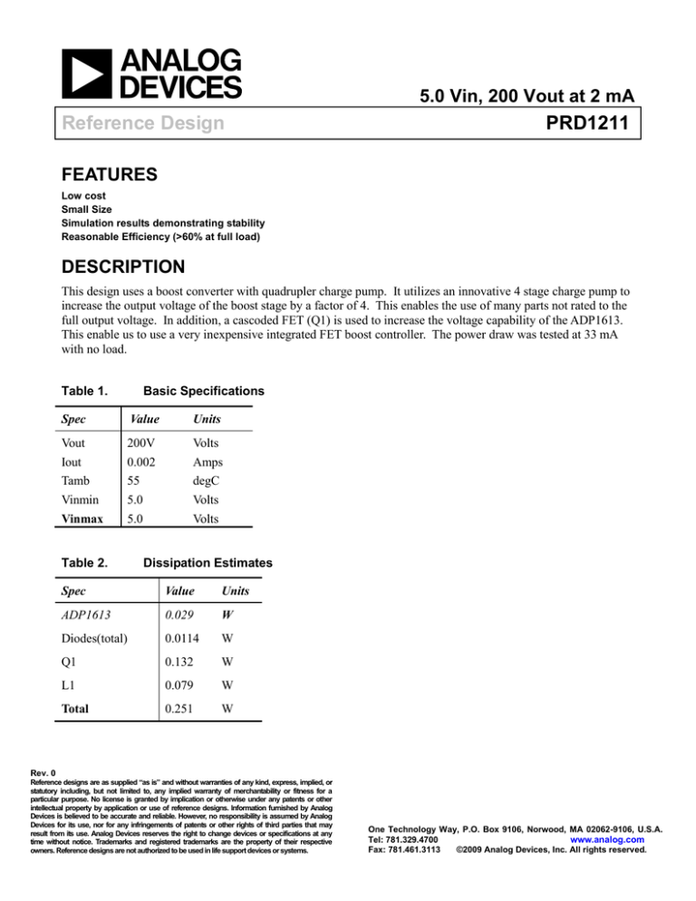
5.0 Vin, 200 Vout at 2 mA Reference Design PRD1211 FEATURES Low cost Small Size Simulation results demonstrating stability Reasonable Efficiency (>60% at full load) DESCRIPTION This design uses a boost converter with quadrupler charge pump. It utilizes an innovative 4 stage charge pump to increase the output voltage of the boost stage by a factor of 4. This enables the use of many parts not rated to the full output voltage. In addition, a cascoded FET (Q1) is used to increase the voltage capability of the ADP1613. This enable us to use a very inexpensive integrated FET boost controller. The power draw was tested at 33 mA with no load. Table 1. Basic Specifications Spec Value Units Vout Iout 200V 0.002 Volts Amps Tamb 55 degC Vinmin 5.0 Volts Vinmax 5.0 Volts Table 2. Dissipation Estimates Spec Value Units ADP1613 0.029 W Diodes(total) 0.0114 W Q1 0.132 W L1 0.079 W Total 0.251 W Rev. 0 Reference designs are as supplied “as is” and without warranties of any kind, express, implied, or statutory including, but not limited to, any implied warranty of merchantability or fitness for a particular purpose. No license is granted by implication or otherwise under any patents or other intellectual property by application or use of reference designs. Information furnished by Analog Devices is believed to be accurate and reliable. However, no responsibility is assumed by Analog Devices for its use, nor for any infringements of patents or other rights of third parties that may result from its use. Analog Devices reserves the right to change devices or specifications at any time without notice. Trademarks and registered trademarks are the property of their respective owners. Reference designs are not authorized to be used in life support devices or systems. One Technology Way, P.O. Box 9106, Norwood, MA 02062-9106, U.S.A. Tel: 781.329.4700 www.analog.com Fax: 781.461.3113 ©2009 Analog Devices, Inc. All rights reserved. Reference Design Table 3. Temperature Estimates Spec Value Units Ambient Temp 55 degC ADP1613 58 degC Diodes(total) 56 degC Q1 67 degC L1 64 degC Table 4. Operational Estimates Spec Value Units Iin (simulation) 0.142 A Irms L1 0.245 A Ipk L1 0.632 A Irms Fet 0.242 A Pk Voltage FET 51 V Table 5. PRD1211 Measured results Spec Value Units Total Loss (Iout =2 mA) 0.257 W Vout ripple RMS 0.025 Vrms Rev. 1 | Page 2 of 8 Reference Design PRD1211 TABLE OF CONTENTS Features ......................................................................................................................................................................1 Description .................................................................................................................................................................1 Revision History .........................................................................................................................................................3 Schematic ...................................................................................................................................................................4 Bill of Materials..........................................................................................................................................................4 Graphs ........................................................................................................................................................................5 TABLE OF FIGURES Figure 1. Boost Converter with Quadrupler Charge Pump Topology ...................................................................4 Figure 2. Bode Plot ...............................................................................................................................................5 Figure 3. Measured Efficiency over Load .............................................................................................................6 Figure 4.......................................................................................................................................................................7 Figure 5.......................................................................................................................................................................7 Figure 6.......................................................................................................................................................................7 REVISION HISTORY 2/18/2010—Revision 1: Initial Version Rev. 1 | Page 3 of 8 Reference Design PRD1211 SCHEMATIC Figure 1. Boost Converter with Quadrupler Charge Pump Topology BILL OF MATERIALS Table 6. Des Bill of Materials MFG Part Number U1 ADI ADP1613ARMZ-R7 L1 Coilcraft ME3220-332 D1 D2 D3 D4 D5 D6 D7 Diodes Inc. Diodes Inc. Diodes Inc. Diodes Inc. Diodes Inc. Diodes Inc. Diodes Inc. Co1 Co2 Co3 Co4 Cbst1 Cbst2 Murata TDK TDK TDK Murata Murata Component Specs Pkg Qty Area (mm^2) Cost* MSOP-8 1 14.70 $0.700 3mm x 3mm x 2mm SOD123 SOD123 SOD123 SOD123 SOD123 SOD123 SOD123 1 8.00 $0.230 1N4148W 1N4148W 1N4148W 1N4148W 1N4148W 1N4148W 1N4148W Integrated Switching Regulator 3.3uH, 138mOhms, 1.7 Apk 150mA ,100V 150mA ,100V 150mA ,100V 150mA ,100V 150mA ,100V 150mA ,100V 150mA ,100V 1 1 1 1 1 1 1 6.5 6.5 6.5 6.5 6.5 6.5 6.5 $0.060 $0.060 $0.060 $0.060 $0.060 $0.060 $0.060 GRM188R72A104K C3216X7R2E104K C3216X7R2E104K C3216X7R2E104K GRM188R72A104K GRM188R72A104K 0.1uF, 100V, 0603, X7R 0.1uF, 250V, 1206, X7R 0.1uF, 250V, 1206, X7R 0.1uF, 250V, 1206, X7R 0.1uF, 100V, 0603, X7R 0.1uF, 100V, 0603, X7R 0603 1206 1206 1206 0603 0603 1 1 1 2 1 1 1.28 5.1 5.1 10.2 1.28 1.28 $0.031 $0.063 $0.063 $0.126 $0.031 $0.031 Rev. 1 | Page 4 of 8 Reference Design Des Cbst3 Cin MFG PRD1211 Part Number Component Specs Pkg Qty Area (mm^2) Cost* 0603 0805 1 1 1.28 2.50 $0.031 $0.012 SOT23-6 1 9.3 $0.66 Q1 Murata Taiyo Yuden Vishay GRM188R72A104K 0.1uF, 100V, 0603, X7R LMK212 1uF, 10V, 805, X7R B7105MG-T Si3458BDV 128 mΩ, 2 9Vth,60 V Cv5 Css Rc1 Cc1 Cc0 Rf1a Murata Vishay Vishay Vishay Vishay Vishay GRM188R61A105K 10% tolerance 5% tolerance 10% tolerance 10% tolerance 1% tolerance 1uF,10V,X5R 100 nF 200 kohm 1.2 nF 10 pF 402 kohm 0603 0402 0402 0402 0402 0805 1 1 1 1 1 1 1.30 0.70 0.70 0.70 0.70 0.70 $0.010 $0.005 $0.005 $0.005 $0.005 $0.005 Rf1b Rf2 Rb0 Vishay Vishay Vishay 1% tolerance 1% tolerance 5% tolerance 422 kohm 5.11 kohm 1 Ohm 0805 0402 0402 Totals 1 1 1 27 0.70 0.70 0.70 112.4 $0.005 $0.005 $0.005 2.448 GRAPHS Figure 2. Bode Plot Rev. 1 | Page 5 of 8 Reference Design PRD1211 Figure 3. Measured Efficiency over Load Efficiency 0.8 0.7 Efficiency 0.6 0.5 0.4 0.3 0.2 0.1 0 0 0.5 1 1.5 2 2.5 Output Current (mA) Rev. 1 | Page 6 of 8 3 3.5 4 Reference Design PRD1211 Figure 4. Figure 5. Figure 6. Rev. 1 | Page 7 of 8 Reference Design PRD1211 NOTES ©2009 Analog Devices, Inc. All rights reserved. Trademarks and registered trademarks are the property of their respective owners. Error! Unknown document property name. Rev. 1 | Page 8 of 8
