Reference Design PRD1140 ADP2301 Reference Design FEATURES
advertisement
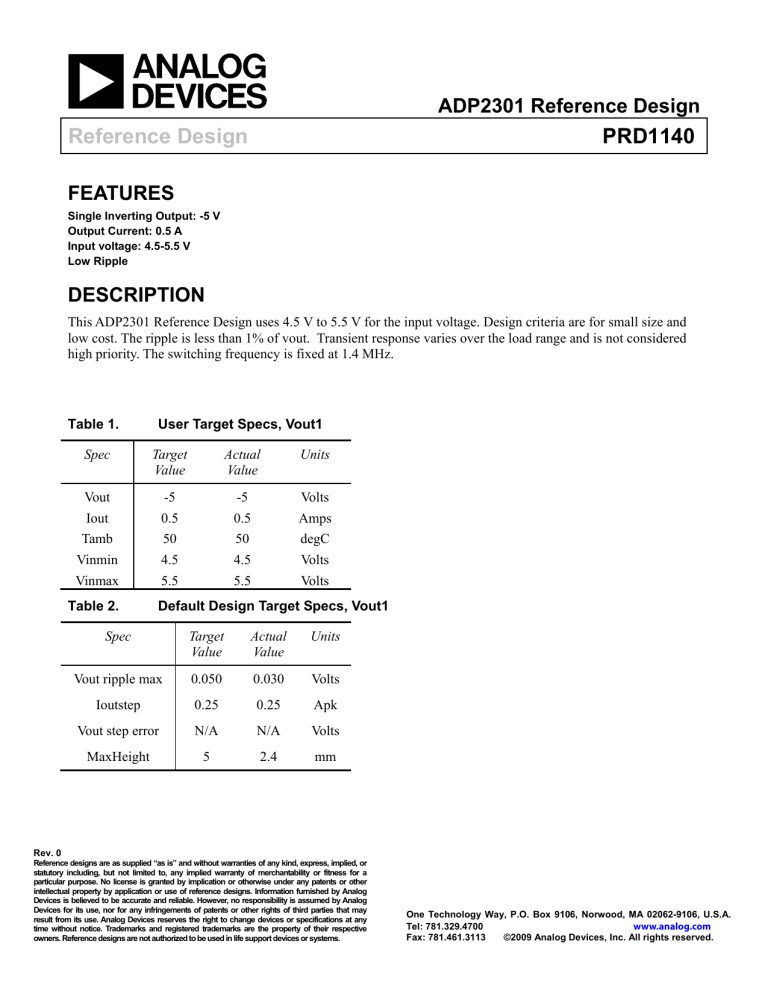
ADP2301 Reference Design Reference Design PRD1140 FEATURES Single Inverting Output: -5 V Output Current: 0.5 A Input voltage: 4.5-5.5 V Low Ripple DESCRIPTION This ADP2301 Reference Design uses 4.5 V to 5.5 V for the input voltage. Design criteria are for small size and low cost. The ripple is less than 1% of vout. Transient response varies over the load range and is not considered high priority. The switching frequency is fixed at 1.4 MHz. Table 1. User Target Specs, Vout1 Spec Target Value Actual Value Units Vout -5 -5 Volts Iout 0.5 0.5 Amps Tamb 50 50 degC Vinmin 4.5 4.5 Volts Vinmax 5.5 5.5 Volts Table 2. Default Design Target Specs, Vout1 Spec Target Value Actual Value Units Vout ripple max 0.050 0.030 Volts Ioutstep 0.25 0.25 Apk Vout step error N/A N/A Volts MaxHeight 5 2.4 mm Rev. 0 Reference designs are as supplied “as is” and without warranties of any kind, express, implied, or statutory including, but not limited to, any implied warranty of merchantability or fitness for a particular purpose. No license is granted by implication or otherwise under any patents or other intellectual property by application or use of reference designs. Information furnished by Analog Devices is believed to be accurate and reliable. However, no responsibility is assumed by Analog Devices for its use, nor for any infringements of patents or other rights of third parties that may result from its use. Analog Devices reserves the right to change devices or specifications at any time without notice. Trademarks and registered trademarks are the property of their respective owners. Reference designs are not authorized to be used in life support devices or systems. One Technology Way, P.O. Box 9106, Norwood, MA 02062-9106, U.S.A. Tel: 781.329.4700 www.analog.com Fax: 781.461.3113 ©2009 Analog Devices, Inc. All rights reserved. Reference Design PRD1140 TABLE OF CONTENTS Features ......................................................................................................................................................................1 Description .................................................................................................................................................................1 Revision History.........................................................................................................................................................2 Schematic ...................................................................................................................................................................3 Bill of Materials..........................................................................................................................................................3 TABLE OF FIGURES Figure 1. Inverting buck boost Schematic.............................................................................................................3 REVISION HISTORY 8/03/2009—Revision 0: Initial Version Rev. 0 | Page 2 of 4 Reference Design PRD1140 SCHEMATIC Figure 1. Inverting buck boost Schematic 4.5-5.5 V Vin Cbst L1 BST SW U1 GND Rfbl Ren ADP2301 FB Cin VIN D1 Cout Vout1 EN Rfbh BILL OF MATERIALS Table 3. Bill of Materials Item # Des Mfg Part Number Component Specs 1 U1 ADI ADP2301 Current Mode Step Down DC/DC Regulator 2 L1 Coilcraft LPS6225-682MLC 6.8uH, 100mOhm 2x2 inductor 3 D1 Diodes Inc. B230A 4 Cin Murata 5 Cout 6 Package Qty Area (mm^2) Height (mm) TSOT-6 1 8.12 1.0 6x6 1 36.0 2.4 Single,2A,30V Schottky SMA 1 16.8 2.3 GRM31CR71C106K 10uF,16V,X7R,2mOhm 1206 1 5.1 1.6 Murata GRM31CR60J226K 22uF,6.3V,X5R,2mOhm 1206 1 5.1 1.6 Cbst Murata GRM188R70J104KA01 100nF,6.3V,X7R 0603 1 1.3 0.8 7 Rfbh Vishay 1% tolerance 22.1kohm 0603 1 1.3 0.5 8 Rfbl Vishay 1% tolerance 4.12kohm 0603 1 1.3 0.5 9 Ren Vishay 1% tolerance 10.0kohm 0603 1 1.3 0.5 9 76.3 2.4 Total: Rev. 0 | Page 3 of 4 Cost Reference Design PRD1140 NOTES ©2009 Analog Devices, Inc. All rights reserved. Trademarks and registered trademarks are the property of their respective owners. Error! Unknow Rev. 0 | Page 4 of 4
