Reference Design PRD01111 ADP1621 28V Boost FEATURES
advertisement
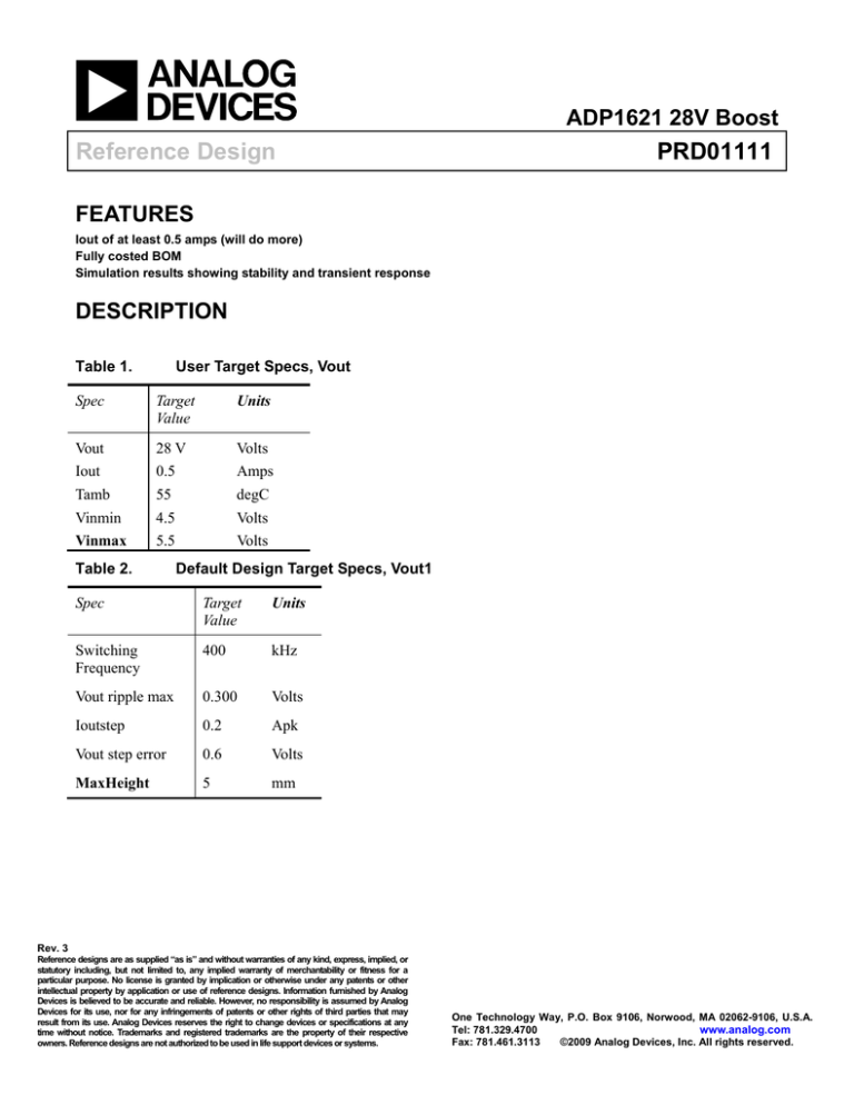
ADP1621 28V Boost Reference Design PRD01111 FEATURES Iout of at least 0.5 amps (will do more) Fully costed BOM Simulation results showing stability and transient response DESCRIPTION Table 1. User Target Specs, Vout Spec Target Value Units Vout 28 V Volts Iout 0.5 Amps Tamb 55 degC Vinmin 4.5 Volts Vinmax 5.5 Volts Table 2. Default Design Target Specs, Vout1 Spec Target Value Units Switching Frequency 400 kHz Vout ripple max 0.300 Volts Ioutstep 0.2 Apk Vout step error 0.6 Volts MaxHeight 5 mm Rev. 3 Reference designs are as supplied “as is” and without warranties of any kind, express, implied, or statutory including, but not limited to, any implied warranty of merchantability or fitness for a particular purpose. No license is granted by implication or otherwise under any patents or other intellectual property by application or use of reference designs. Information furnished by Analog Devices is believed to be accurate and reliable. However, no responsibility is assumed by Analog Devices for its use, nor for any infringements of patents or other rights of third parties that may result from its use. Analog Devices reserves the right to change devices or specifications at any time without notice. Trademarks and registered trademarks are the property of their respective owners. Reference designs are not authorized to be used in life support devices or systems. One Technology Way, P.O. Box 9106, Norwood, MA 02062-9106, U.S.A. Tel: 781.329.4700 www.analog.com Fax: 781.461.3113 ©2009 Analog Devices, Inc. All rights reserved. Reference Design PRD01111 TABLE OF CONTENTS Features ......................................................................................................................................................................1 Description .................................................................................................................................................................1 Revision History .........................................................................................................................................................2 Schematic ...................................................................................................................................................................3 Bill of Materials..........................................................................................................................................................3 Graphs ........................................................................................................................................................................5 TABLE OF FIGURES Figure 1. 4.5 – 5.5 V in, 28 V out at 0.5 A ............................................................................................................3 Figure 2. Full Load Bode Plot ..............................................................................................................................5 Figure 3. Vout Transient Response 200 mA step load ...........................................................................................5 REVISION HISTORY 5/13/2009—Revision 1: Initial Version Rev. 3 | Page 2 of 2 Reference Design PRD01111 SCHEMATIC Figure 1. 4.5 – 5.5 V in, 28 V out at 0.5 A D1 L1 Vin Cin1 Cin2 Vout Cout Rsn Csn Rin1 Rin2 Ren Ccin Enable / Sync SDSN IN GND CS Rs2 U1 COMP Cc1 Rc1 FB GATE FREQ PGND Rfreq RF2 PIN Q1 Rs1 ADP1621ARMZ Cpin Rsense RF1 BILL OF MATERIALS Table 3. Des Bill of Materials MFG Part Number Component Specs Pkg Qty Area Cost (mm^2) 1 U1 ADI 2 L1 ADP1621ARMZ Integrated Switching Regulator MSOP‐10 1 Coilcraft MSS1048‐472NL_ 4.7uH, 12.3mOhms, 5.6 Apk 10.2mm x 10mm x 4.8mm 1 3 D1 ON Semi MBRS540T3G 5A ,40V SMC 1 50.02 0.12 4 Cin TDK C3225X7R1C226M 22uF, 16V, 1210, X7R 1210 1 8 0.18 Rev. 3 | Page 3 of 3 14.7 1.32 0.44 Reference Design Des MFG Part Number PRD01111 Component Specs Pkg Qty Area Cost (mm^2) 5 Cin2 6 Cout Murata GRM31CR71H225K 2.2uF, 50V, 1206, X7R 1206 3 15.4 0.165 7 Q1 Vishay Si4850EY 60 VDS, 48 mOhms SO8 2 62 0.32 8 Rsense Susumu RL1220T‐R010‐J 10 mOhms 0805 2 3.2 0.088 9 Rs1 Vishay 5% tolerance 1 kOhms 0805 1 2.5 0.005 10 Rs2 Vishay 5% tolerance 10 kOhms 0805 1 2.5 0.005 11 Rfreq Vishay 1% tolerance 54.9 kOhms 0805 1 2.5 0.005 12 Rc1 Vishay 5% tolerance 10 kOhms 0805 1 2.5 0.005 13 Cc1 Vishay 10% tolerance 3.6 nF 0805 1 2.5 0.005 14 Rf1 Vishay 1% tolerance 110 kohm 0805 1 2.5 0.005 15 Rf2 Vishay 1% tolerance 4.99 kohm 0805 1 2.5 0.005 16 Rsn No Pop 17 Csn No Pop 18 Ccin Murata GRM188R61A105K 1uF,10V,X5R 0603 1 1.3 0.01 19 Cpin Murata GRM188R61A105K 1uF,10V,X5R 0603 1 1.3 0.01 20 Rin1 Vishay 5% tolerance 154 Ohms 0805 1 2.5 0.005 21 Rin2 Vishay 5% tolerance 154 Ohms 0805 1 2.5 0.005 22 REN Vishay 5% tolerance 50 kOhms 0805 1 2.5 0.005 Totals 23 Electrolytic for stability during testing Rev. 3 | Page 4 of 4 178.4 2.698 Reference Design PRD01111 GRAPHS Figure 2. Figure 3. Full Load Bode Plot Vout Transient Response (200 mA step load from full load) Rev. 3 | Page 5 of 5 Reference Design PRD01111 ©2009 Analog Devices, Inc. All rights reserved. Trademarks and registered trademarks are the property of their respective owners. Error! Unknow Rev. 3 | Page 6 of 6
