AN-1225 APPLICATION NOTE
advertisement
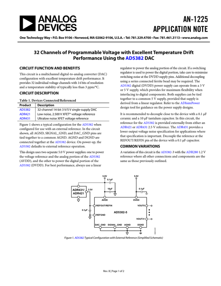
AN-1225 APPLICATION NOTE One Technology Way • P.O. Box 9106 • Norwood, MA 02062-9106, U.S.A. • Tel: 781.329.4700 • Fax: 781.461.3113 • www.analog.com 32 Channels of Programmable Voltage with Excellent Temperature Drift Performance Using the AD5382 DAC CIRCUIT FUNCTION AND BENEFITS regulator to power the analog portion of the circuit. If a switching regulator is used to power the digital portion, take care to minimize switching noise at the DVDD supply pins. Additional decoupling using a series connected ferrite bead may be required. The AD5382 digital (DVDD) power supply can operate from a 3 V or 5 V supply, which provides for maximum flexibility when interfacing to digital components. Both supplies can be tied together to a common 5 V supply, provided that supply is derived from a linear regulator. Refer to the ADIsimPower design tool for guidance on the power supply designs. This circuit is a multichannel digital-to-analog converter (DAC) configuration with excellent temperature drift performance. It provides 32 individual voltage channels with 14 bits of resolution and a temperature stability of typically less than 3 ppm/°C. CIRCUIT DESCRIPTION Table 1. Devices Connected/Referenced Product AD5382 ADR421 ADR431 Description 32-channel 14-bit 3 V/5 V single-supply DAC Low noise, 2.500 V XFET® voltage reference Ultralow noise XFET voltage reference It is recommended to decouple close to the device with a 0.1 µF ceramic and a 10 µF tantalum capacitor. In this circuit, the reference for the AD5382 is provided externally from either an ADR421 or ADR431 2.5 V reference. The ADR431 provides a lower output voltage noise specification for applications where that specification is important. Decouple the reference at the REFOUT/REFIN pin of the device with a 0.1 µF capacitor. Figure 1 shows a typical configuration for the AD5382 when configured for use with an external reference. In the circuit shown, all AGND, SIGNAL_GND, and DAC_GND pins are tied together to a common AGND. AGND and DGND are connected together at the AD5382 device. On power-up, the AD5382 defaults to external reference operation. COMMON VARIATIONS A variation of this circuit is the AD5382-3 with the ADR280 1.2 V reference where all other connections and components are the same as those previously outlined. This design uses two separate 5.0 V power supplies: one to power the voltage reference and the analog portion of the AD5382 (AVDD), and the other to power the digital portion of the AD5382 (DVDD). For best performance, always use a linear 5.0V 5.0V 0.1µF ADR431/ ADR421 10µF 2.5V 0.1µF AVDD DVDD VOUT0 REFOUT/REFIN 0.1µF AD5382-5 REFGND VOUT31 SIGNAL_GND AGND DGND 08203-001 DAC_GND Figure 1. AD5382 Typical Configuration with External Reference (Simplified Schematic) Rev. B | Page 1 of 2 AN-1225 Application Note LEARN MORE Data Sheets and Evaluation Boards ADIsimPower Design Tool. AD5382 Data Sheet. Kester, Walt. 2005. The Data Conversion Handbook. Analog Devices. Chapters 3 and 7. AD5382 Evaluation Board. MT-015 Tutorial, Basic DAC Architectures II: Binary DACs. Analog Devices. ADR431 Data Sheet. MT-031 Tutorial, Grounding Data Converters and Solving the Mystery of AGND and DGND. Analog Devices. 5/13—Rev. A to Rev. B MT-101 Tutorial, Decoupling Techniques. Analog Devices. Voltage Reference Wizard Design Tool. ADR421 Data Sheet. REVISION HISTORY Document Title Changed from CN-0011 to AN-1225 ....... Universal 5/09—Rev. 0 to Rev. A Updated Format .................................................................. Universal 10/08—Revision 0: Initial Version ©2008–2013 Analog Devices, Inc. All rights reserved. Trademarks and registered trademarks are the property of their respective owners. D08203-0-5/13(B) Rev. B | Page 2 of 2
