CIRCUIT FUNCTION AND BENEFITS
temperature coefficients of the DAC. This approach is recommended in circuits where gains of greater than 1 are required.
In applications where the DAC output voltage range is required
to be larger than the input voltage, a programmable gain circuit
can be used. This circuit provides a programmable gain
function using a multiplying DAC, the AD5450/AD5451/
AD5452/AD5453, and a fast, low offset operational amplifier,
the AD8065. The maximum gain value and the temperature
coefficient are set by external resistors, and the resolution of the
programmable gain is set by the resolution of the DAC.
VOUT = –Gain × VIN ×
D
2N
(1)
where D is the digital word loaded to the DAC. D = 0 to 255
(8-bit AD5450), D = 0 to 1023 (10-bit AD5451), D = 0 to 4095
(12-bit AD5452), D = 0 to 16383 (14-bit AD5453); N is the
number of bits.
The key benefit of this circuit is its ability to overcome gain TC
errors using resistor matching. The TC of the external resistors
needs to match each other but do not need to match that of the
DAC internal ladder resistance.
CIRCUIT DESCRIPTION
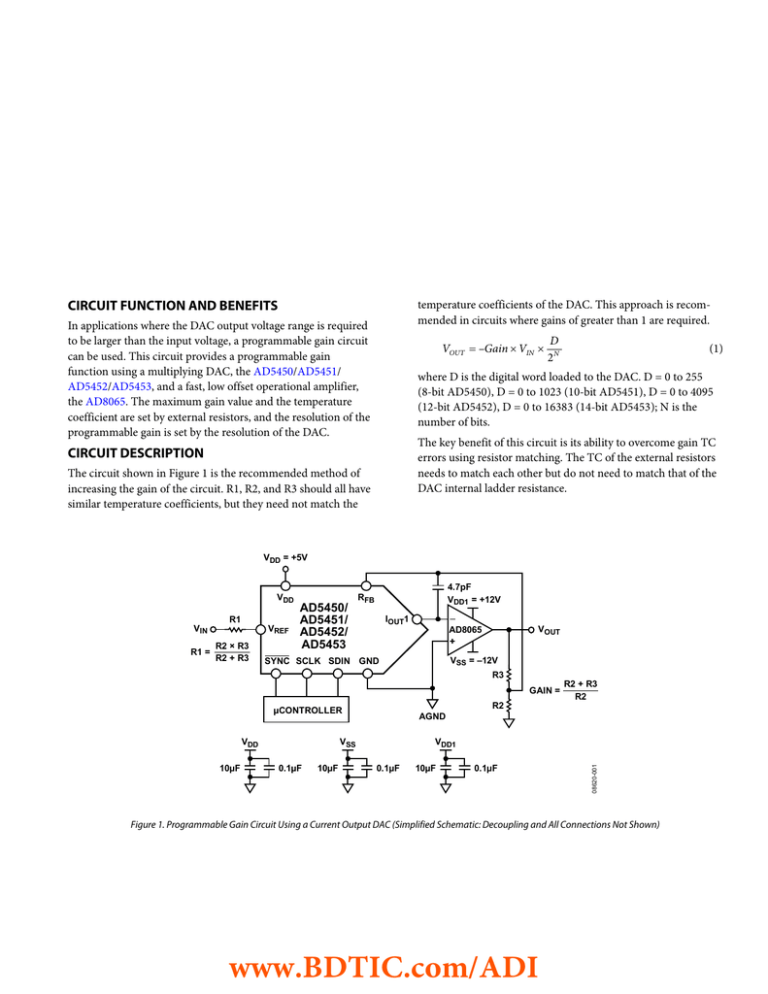
The circuit shown in Figure 1 is the recommended method of
increasing the gain of the circuit. R1, R2, and R3 should all have
similar temperature coefficients, but they need not match the
VDD = +5V
VIN
R1
VREF
R2 × R3
R1 =
R2 + R3
AD5450/
AD5451/
AD5452/
AD5453
4.7pF
VDD1 = +12V
RFB
IOUT1
VOUT
AD8065
VSS = –12V
SYNC SCLK SDIN GND
R3
GAIN =
µCONTROLLER
VSS
VDD
10µF
AGND
0.1µF
10µF
R2
R2 + R3
R2
VDD1
0.1µF
10µF
0.1µF
08620-001
VDD
Figure 1. Programmable Gain Circuit Using a Current Output DAC (Simplified Schematic: Decoupling and All Connections Not Shown)
www.BDTIC.com/ADI
Resistor R1 is required because R1 plus the input impedance of
the DAC must equal the total feedback resistance which is RFB
plus R2||R3. The input impedance of the DAC is RFB, so
R1 + RFB = RFB + R2||R3
(2)
R1 = R2||R3
(3)
The values of R1 and R2 must be chosen such that the output
voltage does not exceed the output range of the operational
amplifier for the given supply voltage. Also note that the bias
current of the operational amplifier is multiplied by the total
feedback resistance (RFB + R2||R3) to give an associated offset.
Thus, the values of R1 and R2 cannot be too large or they will
have a significant effect on the overall offset voltage.
The AD5450/AD5451/AD5452/AD5453 products are designed
on a 5 V CMOS process and operate from a VDD1 power supply
of 2.5 V to 5.5 V. The output amplifier is driven from a dual
power supply voltage (VDD/VSS), which needs to be large enough
to accommodate the analog output range of the circuit.
Generally, ±12 V supplies are sufficient. The 4.7 pF capacitor is
used to prevent ringing or instability in the closed-loop
application.
The input offset voltage of an op amp is multiplied by the
variable noise gain (due to the code-dependent output
resistance of the DAC) of the circuit. A change in this noise gain
between two adjacent digital codes produces a step change in
the output voltage due to the amplifier’s input offset voltage.
This output voltage change is superimposed on the desired
change in output between the two codes and produces a differential linearity error, which if large enough, could cause the DAC
to be non-monotonic. The AD8065 benefits from both a low input
offset voltage and low bias currents to overcome this issue.
COMMON VARIATIONS
LEARN MORE
ADIsimPower Design Tool. Analog Devices.
Kester, Walt. The Data Conversion Handbook. Chapter 3, 7.
Analog Devices. 2005.
MT-015 Tutorial, Basic DAC Architectures II: Binary DACs.
Analog Devices.
MT-031 Tutorial, Grounding Data Converters and Solving the
Mystery of “AGND” and “DGND.” Analog Devices.
MT-033 Tutorial, Voltage Feedback Op Amp Gain and
Bandwidth. Analog Devices.
MT-035 Tutorial, Op Amp Inputs, Outputs, Single-Supply, and
Rail-to-Rail Issues. Analog Devices.
MT-101 Tutorial, Decoupling Techniques. Analog Devices.
Voltage Reference Wizard Design Tool. Analog Devices.
Data Sheets
AD5450 Data Sheet
AD5451 Data Sheet
AD5452 Data Sheet
AD5453 Data Sheet
AD8065 Data Sheet
OP1177 Data Sheet
REVISION HISTORY
11/09—Rev. 0 to Rev. A
Updated Format .................................................................. Universal
1/09—Revision 0: Initial Version
The OP1177 is another excellent op amp candidate for the I-V
conversion circuit. It also provides low offset voltage and
ultralow bias current. For the selection of the reference, the
input voltage is restricted by the rail-to-rail voltage of the
operational amplifier selected and also the gain set up by the
resistors R2 and R3.
(Continued from first page) "Circuits from the Lab" are intended only for use with Analog Devices products and are the intellectual property of Analog Devices or its licensors. While you may
use the "Circuits from the Lab" in the design of your product, no other license is granted by implication or otherwise under any patents or other intellectual property by application or use of
the "Circuits from the Lab". Information furnished by Analog Devices is believed to be accurate and reliable. However, "Circuits from the Lab" are supplied "as is" and without warranties of any
kind, express, implied, or statutory including, but not limited to, any implied warranty of merchantability, noninfringement or fitness for a particular purpose and no responsibility is assumed
by Analog Devices for their use, nor for any infringements of patents or other rights of third parties that may result from their use. Analog Devices reserves the right to change any "Circuits
from the Lab" at any time without notice, but is under no obligation to do so. Trademarks and registered trademarks are the property of their respective owners.
©2009 Analog Devices, Inc. All rights reserved. Trademarks and
registered trademarks are the property of their respective owners.
CN08620-0-11/09(A)
www.BDTIC.com/ADI
