AN-1041 APPLICATION NOTE
advertisement
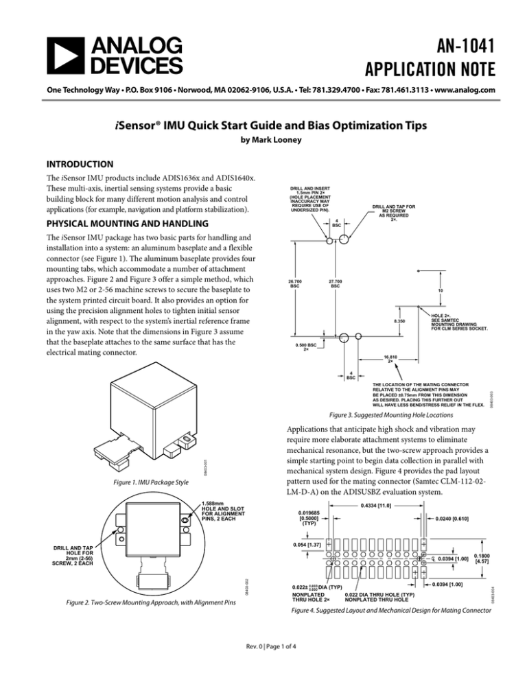
AN-1041 APPLICATION NOTE One Technology Way • P.O. Box 9106 • Norwood, MA 02062-9106, U.S.A. • Tel: 781.329.4700 • Fax: 781.461.3113 • www.analog.com iSensor® IMU Quick Start Guide and Bias Optimization Tips by Mark Looney INTRODUCTION The iSensor IMU products include ADIS1636x and ADIS1640x. These multi-axis, inertial sensing systems provide a basic building block for many different motion analysis and control applications (for example, navigation and platform stabilization). DRILL AND INSERT 1.5mm PIN 2× (HOLE PLACEMENT INACCURACY MAY REQUIRE USE OF UNDERSIZED PIN). PHYSICAL MOUNTING AND HANDLING DRILL AND TAP FOR M2 SCREW AS REQUIRED 2×. 4 BSC The iSensor IMU package has two basic parts for handling and installation into a system: an aluminum baseplate and a flexible connector (see Figure 1). The aluminum baseplate provides four mounting tabs, which accommodate a number of attachment approaches. Figure 2 and Figure 3 offer a simple method, which uses two M2 or 2-56 machine screws to secure the baseplate to the system printed circuit board. It also provides an option for using the precision alignment holes to tighten initial sensor alignment, with respect to the system’s inertial reference frame in the yaw axis. Note that the dimensions in Figure 3 assume that the baseplate attaches to the same surface that has the electrical mating connector. 26.700 BSC 27.700 BSC 10 8.350 HOLE 2×. SEE SAMTEC MOUNTING DRAWING FOR CLM SERIES SOCKET. 0.500 BSC 2× 16.810 2× THE LOCATION OF THE MATING CONNECTOR RELATIVE TO THE ALIGNMENT PINS MAY BE PLACED ±0.75mm FROM THIS DIMENSION AS DESIRED. PLACING THIS FURTHER OUT WILL HAVE LESS BEND/STRESS RELIEF IN THE FLEX. 08403-003 4 BSC Figure 3. Suggested Mounting Hole Locations 08403-001 Applications that anticipate high shock and vibration may require more elaborate attachment systems to eliminate mechanical resonance, but the two-screw approach provides a simple starting point to begin data collection in parallel with mechanical system design. Figure 4 provides the pad layout pattern used for the mating connector (Samtec CLM-112-02LM-D-A) on the ADISUSBZ evaluation system. Figure 1. IMU Package Style 1.588mm HOLE AND SLOT FOR ALIGNMENT PINS, 2 EACH 0.4334 [11.0] 0.019685 [0.5000] (TYP) 0.054 [1.37] 08403-002 0.0394 [1.00] 0.022± DIA (TYP) NONPLATED 0.022 DIA THRU HOLE (TYP) NONPLATED THRU HOLE THRU HOLE 2× 0.1800 [4.57] 0.0394 [1.00] Figure 4. Suggested Layout and Mechanical Design for Mating Connector Rev. 0 | Page 1 of 4 08403-004 DRILL AND TAP HOLE FOR 2mm (2-56) SCREW, 2 EACH Figure 2. Two-Screw Mounting Approach, with Alignment Pins 0.0240 [0.610] AN-1041 Application Note IMU INSTALLATION AND REMOVAL SPI INTERFACE IMU installation follows a two-step sequence: Table 2 provides a list of typical configuration settings that master processors require for SPI communication with iSensor IMUs. These settings are normally in control registers. For example, the SPI_BAUD, SPI_CTL, and SPI_FLG registers serve this purpose in the ADSP-BF533 processor family. 1. 2. Secure the baseplate using machine screws. Press the connector into its mate. For removal, gently pry the connector from its mate, using a small slot screwdriver. Then, remove the screws and lift the part up. Never attempt to unplug the connector by pulling on the plastic case or baseplate. While very reliable in normal operation, the flexible connector can break when subjected to unreasonable handling. When broken, there are no repair options for the flexible connector. ELECTRICAL HOOK-UP When power is applied, the iSensor products start up and begin producing data, independent of user inputs. Figure 5 provides a hook-up diagram, which accommodates power, ground, four serial signals, and a data-ready signal. The data-ready signal typically drives an interrupt service routine in the master processor, which ensures data coherency while optimizing processor resources. I/O LINES ARE COMPATIBLE WITH 3.3V OR 5V LOGIC LEVELS 10 11 12 ADIS1636x/ ADIS1640x SS 6 CS SCLK 3 SCLK MOSI 5 DIN MISO 4 DOUT IRQ 7 DIO1 SPI SLAVE 14 15 08430-005 13 Processor Setting Master SCLK Rate ≤ 2 MHz SPI Mode 3 MSB-First Mode 16-Bit Mode Data communication requires firmware-level register management. Placing a command on DIN involves writing to the transmit buffer register (SPI_TDBR in the ADSP-BF533). Acquiring output data from DOUT involves reading the receive buffer register (SPI_RDBR in the ADSP-BF533). OPTIMIZING BIAS ACCURACY AND STABILITY 1. 2. Figure 5. Electrical Hook-Up Diagram Table 1. Generic Master Processor Pin Names and Functions Pin Name SS IRQ MOSI MISO SCLK Function Slave select Interrupt request Master output, slave input Master input, slave output Serial clock Description The iSensor IMUs operate as slaves. Normal mode, SMPL_PRD[7:0] ≤ 0x09. CPOL = 1 (polarity), CHPA = 1 (phase). Bit sequence. Shift register/data length. All of the iSensor IMUs include a factory calibration that provides substantial improvements in bias accuracy over most MEMS gyroscopes. Some environmental conditions (such as temperature cycling and installation) can cause minor shifts in gyroscope output bias. A single-point adjustment can address these shifts and restore the entire calibration, including the temperature correction that comes with some parts. This involves measuring the zero-rotation gyroscope output and writing the opposite value into its offset register. There are three basic options for executing the single-point adjustment in the gyroscopes: autonull, precision autonull, and manual calibration. The following conditions/settings help assure optimum accuracy during this process: 5V VDD SYSTEM PROCESSOR SPI MASTER Table 2. Generic Master Processor SPI Settings 3. Rev. 0 | Page 2 of 4 Sample rate = 819.2 SPS (SMPL_PRD[7:0] = 0x01) Thermal stability Reading the temperature output registers can help determine when this happens. Zero rotation (including vibration) Take a small sample of data and make sure that the output noise is in agreement with the data sheet. For example, with no filtering, the ADIS1636x and ADIS1640x should have less than 1°/sec rms of noise on their gyroscopes. Application Note AN-1041 Averaging multiple samples of each gyroscope helps address the uncertainty associated with gyroscope noise. The Allan variance curve provides a relationship between averaging time and bias accuracy. Manual calibration offers the advantage of optimizing the bias accuracy for applications that can accommodate the extended averaging times. In reviewing the Allan variance curve (see Figure 6), a 100 second average time yields the best accuracy for a given population of parts. Use the following steps to achieve the best manual calibration results: 1. 2. +1σ 0.01 MEAN 3. 4. 5. 6. –1σ 0.001 0.1 1 10 100 1k 10k Tau (sec) 08403-006 ROOT ALLAN VARIANCE (°/sec) 0.1 Manual Calibration Figure 6. ADIS1636x/ADIS1640x Allan Variance Curve Autonull Function The autonull function automatically reads each gyroscope output register and writes the opposite value into the appropriate user offset register. Use the following steps to obtain the best results from this option: 1. 2. 3. 4. SMPL_PRD[7:0] = 0x01 (DIN = 0xB601) SENS_AVG[7:0] = 0x06 (DIN = 0xB806) Allow 200 ms for the internal filter taps to fill up. GLOB_CMD[0] = 1 (DIN = 0xBE01) When using this sequence, the equivalent averaging time is approximately 0.15 seconds. According to Figure 6, this produces a bias accuracy of approximately 0.08°/sec. 7. 8. SMPL_PRD[7:0] = 0x01 (DIN = 0xB601) Wait 1 min to 2 min for initial thermal settling. This may be application-dependent and require warm-up periods up to 10 min to 15 min. Verify by reading the TEMP_OUT registers. Read 82,000 samples at 819.2 SPS (~100 seconds) Calculate the average of these values. Convert this estimate into an offset correction factor. For the internal user-offset registers: a. Multiply the estimate by 80. b. Round it to the nearest integer. c. Convert the number to a 14-bit, twos complement format. Write it to the appropriate user-offset register. GLOB_CMD[3] = 1 (DIN = 0xBE04), if using the internal user-offset correction registers. The user-offset registers offer a resolution step size of 0.0125°/sec, which is sufficient for a large majority of applications. For those who have the opportunity to perform the correction in their processor, users can achieve incremental performance gains and increase the number of parts that perform to the 0.006°/sec bias accuracy shown in Figure 6. In this case, use a 16-bit register that adds to the IMU gyroscope outputs and change the multiplication factor in Step 6a from 80 to 320. Sample Rate Decimation Precision Autonull Function The precision autonull function offers better accuracy than the autonull function by taking a 30 second average of each gyroscope output, then calculating the appropriate correction factors and automatically loading them into the user-offset register. During the 30 second measurement period, the IMU automatically sets its sample rate and filters for optimal data collection. For the ADIS1636x and ADIS1640x families, the bias correction accuracy can approach 0.008°/sec (see Figure 6, 30 second average time). Execute this function by setting GLB_ CMD[4] = 1 (DIN = 0xBE10). The internal sample rate of 819.2 SPS is essential to preserving the best bias stability performance in these products. For applications that value lower sample rates, use the internal Bartlett window filters to limit the bandwidth and decimate the data available in the gyroscope and accelerometer output registers. One method is to use the data-ready output to drive a counter, which divides the system-level sample rate by integer levels. While each system may require specific tuning, use the number of taps per stage in the Bartlett window filter as the maximum division factor in each setup. For example, if SENS_AVG[2:0] = 100, which translates to 16 taps per stage, users can divide the sample rate by any integer number between 2 and 16 and still preserve optimum bias stability performance. Rev. 0 | Page 3 of 4 AN-1041 Application Note NOTES ©2009 Analog Devices, Inc. All rights reserved. Trademarks and registered trademarks are the property of their respective owners. AN08403-0-8/09(0) Rev. 0 | Page 4 of 4
