Document 11129469
advertisement

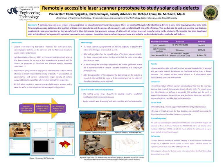
Remotely accessible laser scanner prototype to study solar cells defects Pranav Ram Kamarajugadda, Chetana Bayas, Faculty Advisors: Dr. Richard Chiou, Dr. Michael G Mauk Department of Engineering Technology, Division of Engineering Management and Technology, College of Engineering, Drexel University Summary: A portable, low-­‐cost laser system is being explored for educa9onal and research purposes. Here, we employ this system for iden9fying defects in solar cells. In polycrystalline solar cells, for example, one can determine the loca9on of these grain boundaries and the degree of granularity, and correlate it with the cell’s efficiency. This module can be used as a learning tool that can supplement classroom learning for the Manufacturing Materials course that presents samples of solar cells at various stages of manufacturing to the students. The module has been developed with an inten9on of being remotely operated to enhance and empower the online-­‐classroom learning experience and help the students beCer understand solar cell defects. Introduc9on Methodology • Despite ever-­‐improving fabrica3on methods for semi-­‐conductors, • Light Beam Induced Current (LBIC) is a common tes3ng method, where a The laser scanner plate moves in steps such that the en?re scan takes light beam rasters the surface of the semiconductor material and the coordinates. [1] polycrystalline and contain substan3ally larger density of defects • As each step of the rastering is performed, the current generated by the MATLAB Arduino UNO, Stepper Laser Scanner Module Motors and Driver, Laser Arduino IDE Results posi?ons. The current outputs when ploRed in 3 dimensional space imported into MATLAB to make a 3 dimensional plot of the defects/ approximately locate the disturbances. disturbance posi?ons on the solar cell. Conclusion • A working module of laser scanner was developed that may be used as a learning tool to study the granular defects of solar cells. The results prove Student Benefits and skills improvement that iden?fica?on of defects is successful. This module can be used by students in classroom to operate on and familiarize themselves with three popular pla>orms, LabVIEW, MATLAB and Arduino. • Equips students with developing skills with LabVIEW, MATLAB and Arduino Data Processing/ Analysis using MATLAB Computer with externally induced disturbance, an insula?ng ball of tape, at known modifica?ons to troubleshoo?ng issues Data Acquisi3on using NI DAQ/ LabVIEW Data Processing/ Analysis post processing. • The tes?ng phase helps students to develop crea?ve solu?ons/ Arduino-­‐ controlled laser raster system LabVIEW • A polycrystalline solar cell with a lot of granular irregulari?es is scanned • An LBIC setup consists of a monochroma3c light source, a raster tool to NI DAQ (USB-­‐6211) cell is recorded via the NI DAQ on LabVIEW and stored in a text file for • ANer the comple?on of the rastering, the data stored on the text file is compared to single-­‐crystal PVs, which makes tes3ng them impera3ve. move the wafer, a data acquisi3on and a data processing system. Data Collec3on place in seven steps. • Photovoltaics (PVs) consist of large planar semiconductor surfaces whose efficiency is directly related to the density of defects. [2] Low-­‐cost PVs are SoIware ac?on of rastering on an area of 36 sq. mm. • Solar cells are placed on the movable plate of the laser scanner module. current so generated is measured and mapped against respec3ve Hardware • The laser scanner is programmed, on Arduino pla>orm, to perform the crystallographic defects can be common and the fabricated structures usually require to be tested. Project Requirement Future Work • Development of a tool to support data collec?on and post processing • Develop a Virtual Network for two loca?ons, for remotely accessing this device to enhance the online classroom community Acknowledgement This work was supported by the US Department of Educa3on under joint DHSIP Program with University of Texas at El Paso, PR/Award No.: P031S120131 and by US Na3onal Science Founda3on TUES Grant 1044708 and NSF DUE Award 1245872. The authors wish to express Figure 2: Experimental setup Figure 3: Students performing a test raster sincere gra3tude for their financial support. References [1] Santo Mar3nuzzi and Michael Stemmer “Mapping of defects and their recombina3on strength by a light-­‐beam induced current in silicon wafers”, Material Science and Engineering,Volume 24,Issues 1-­‐3,May 1994, Pages 152–158 [2] Inves3gación y Desarrollo. "Defects in solar cells made of silicon iden3fied." ScienceDaily. ScienceDaily, 2 January 2015 Figure 1: Proposed LBIC Lab setup Figure 4: (leN) Solar cell with external disturbance. (right) A waterfall plot of the current values detect the external disturbance in approximately the correct loca?ons


