Chapter 3. Focused Beam Fabrication Ion
advertisement
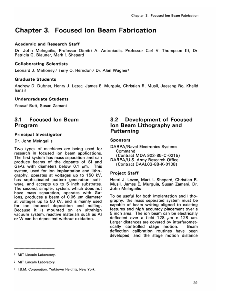
Chapter 3. Focused Ion Beam Fabrication Chapter 3. Focused Ion Beam Fabrication Academic and Research Staff Dr. John Melngailis, Professor Dimitri A. Antoniadis, Professor Carl V. Thompson III, Dr. Patricia G. Blauner, Mark I. Shepard Collaborating Scientists Leonard J. Mahoney,1 Terry 0. Herndon, 2 Dr. Alan Wagner3 Graduate Students Andrew D. Dubner, Henry J. Lezec, James E. Murguia, Christian R. Musil, Jaesang Ro, Khalid Ismail Undergraduate Students Yousaf Butt, Susan Zamani 3.1 Focused Ion Beam Program Principal Investigator Dr. John Melngailis Two types of machines are being used for research in focused ion beam applications. The first system has mass separation and can produce beams of the dopants of Si and GaAs with diameters below 0.1 um. This system, used for ion implantation and lithography, operates at voltages up to 150 kV, has sophisticated pattern generation software, and accepts up to 5 inch substrates. The second, simpler, system, which does not have mass separation, operates with Ga* ions, produces a beam of 0.06 ym diameter at voltages up to 50 kV, and is mainly used for ion induced deposition and milling. Because it is mounted on an ultrahigh vacuum system, reactive materials such as Al or W can be deposited without oxidation. 1 MIT Lincoln Laboratory. 2 MIT Lincoln Laboratory. 3 I.B.M. Corporation, Yorktown Heights, New York. 3.2 Development of Focused Ion Beam Lithography and Patterning Sponsors DAR PA/Naval Electronics Systems Command (Contract MDA 903-85-C-0215) DARPA/U.S. Army Research Office (Contract DAAL03-88-K-0108) Project Staff Henri J. Lezec, Mark I. Shepard, Christian R. Musil, James E. Murguia, Susan Zamani, Dr. John Melngailis To be useful for both implantation and lithography, the mass separated system must be capable of beam writing aligned to existing features and high accuracy placement over a 5 inch area. The ion beam can be electrically deflected over a field 128 ym x 128 jim. Larger distances are covered by interferometrically controlled stage motion. Beam deflection calibration routines have been developed, and the stage motion distance Chapter 3. Focused Ion Beam Fabrication calibration and axis non-orthogonality has been corrected using wafers with known, accurate patterns. Alignment to existing features on a wafer is carried out by imaging the features in the scanning ion microscope mode and by accurately locating the features in the center of the deflection field by means ++ of stage displacement. Using Be ions of 260 keV energy, 60 nm wide lines have been exposed in PMMA 300 nm thick. After development, these lines, which have nearly vertical sidewalls, have proven to be useful for the fabrication of ultrafine feature x-ray lithography masks. See figure 1. Focused Ion Beam Lithography: Focused Ion Beam Lithography: Electroplated Features Ion Beam M //A PMMA/ ,-- Gold Develop & Plate S0.3 im Dissolve PMMA is used to fabricate gold features 50 nm wide and Figure 1. Focused ion beam lithography and gold electroplating ion exposure with a beam of 280 KeV Be++ ions After base. gold plating 200 nm high. PMMA is spun over a thin 2 and gold is electroplated up into the submicron to a dose of about 2.5 x 10¹³ ions/cm , the PMMA is developed, These structures, which will be used for x-ray shown. structure the features. The PMMA is then dissolved leaving Yen, K. Ismail, Y.C. Ku, J. Carter, and H.I. A.T. W. Chu, lithography masks, were fabricated in collaboration with Smith. 30 RLE Progress Report Number 131 Chapter 3. Focused Ion Beam Fabrication 3.3 Frequency Tunable Gunn Diodes Fabricated by Focused Ion Beam Implantation Sponsors DARPA/Naval Electronics Systems Command (Contract MDA 903-85-C-0215) DARPA/U.S. Army Research Office (Contract DAAL03-88-K-01 08) Project Staff Henry J. Lezec, Khalid Ismail, Mark I. Shepard, Leonard J. Mahoney, Professor Dimitri A. Antoniadis, Dr. John Melngailis Gunn diodes have been fabricated by implanting a gradient of doping along the surface between the two contacts. When bias is applied, the electric field in the conduction region varies as a function of distance, and the distance that a Gunn domain can travel is a function of bias. Thus the oscillation frequency can be tuned with bias. We have shown tunability from 6 to 23 GHz as the bias was changed by 12 volts. A Gunn diode with uniform doping shows very little change in frequency as the bias is varied. The device has been modelled to determine the optimum lateral doping gradient profile which would yield the largest These tunable Gunn frequency variation. diodes may prove to be useful in a number of applications including in collision avoidance radar. 3.4 Field-Effect Transistors with Focused Ion Beam Implanted Channel Regions Sponsors DARPA/Naval Electronics Systems Command (Contract MDA 903-85-C-0215) DARPA/U.S. Army Research Office (Contract DAAL03-88-K-0108) Project Staff James E. Murguia, Christian R. Musil, Henry J. Lezec, Professor Dimitri A. Antoniadis, Dr. John Melngailis Preliminary experiments in which GaAs MESFETs were focused-ion-beam implanted with a lateral gradient of doping between the source and drain showed asymmetrical characteristics with some marginal improvements in performance in one direction compared to uniformly doped control devices. These devices had 1 ym gate lengths. The improvements are likely to be more significant if the gate length is in the submicrometer regime. Since, as described in 3.1, " Focused Ion Beam Program" on page 29, our machine is now capable of writing with higher accuracy, we can fabricate submicron devices. In silicon, wafers have been prepared by conventional fabrication up to the point of channel implant. These implants will be carried out with the focused ion beam with boron or arsenic ions. 3.5 Microstructure and Properties of Gold Films Produced by Ion Induced Deposition Sponsors U.S. Army Research Office (Contract DAAL03-87-K-0126) Charles Stark Draper Laboratory Project Staff Jaesang Ro, Dr. Patricia G. Blauner, Yousaf Butt, Professor Carl V. Thompson III, Dr. John Melngailis Material deposition can be produced by using incident ions to break up adsorbed gas molecules. If the gas is dimethyl gold hexafluoro acetylacetonate (C7 H7 F60 2Au), gold is deposited. This form of deposition, when carried out with a focused ion beam, is useful in repairing clear defects in photo and x-ray lithography masks and integrated circuits. Using transmission electron microscopy, we have examined the films grown by this process. In the case of Ar ions from a broad beam generated by an ion implanter and Ga ions from a scanned focused ion beam, the films grown at room temperature consist of isolated hemispherical islands of 60-100 nm diameter. Auger analysis shows the films to contain 30-50 percent carbon in Chapter 3. Focused Ion Beam Fabrication addition to the gold. Deposition at temperatures above 100 degrees C yields films with less than 10 percent carbon and a connected polycrystalline structure. The resistivity of these films is near the bulk value for gold while the films deposited at room temperature have resistivities 200 to 500 times higher. The microstructure also depends on the growth rate that is determined by local gas pressure and the ion current density. 3.6 Focused Ion Beam Induced Depostion of Submicrometer Structures Sponsors U.S. Army Research Office (Contract DAAL03-87-K-01 26) Charles Stark Draper Laboratory Project Staff Dr. Patricia G. Blauner, Jaesang Ro, Yousaf Butt, Professor Carl V. Thompson Ill, Dr. John Melngailis Focused ion beam induced deposition is being used for repairing clear defects in commercial photolithography masks. This technique is expected to be used as well for repairing x-ray lithography masks and also for repairing and local restructuring of integrated circuits. Using a scanned beam of 60 nm diameter and a local gas ambient of (C7 H7F60 2Au), lines of 0.1 pm width have been written. In addition, patches 3 x 3 pm, 1 pm thick with steep side walls have been Typical deposition times are produced. 20-100 sec. per 1 pm 3, depending on beam diameter. Some of these features have been deposited on actual x-ray lithography masks and replicated in resist at the Fraunhofer Institute in Berlin. The lines have been deposited across metal contact fingers and the resistivity has been measured as 500 to 1000 p~)cm (bulk gold measures 2.5 p~ cm). Even at these values, however, local conductors can be fabricated for integrated circuit repair. We have installed a heated stage which is expected to permit deposition of lower resistivity films. Films of tungsten 32 RLE Progress Report Number 131 have also been deposited from a gas of WF 6, and films of Al from organometallic gases will also be tried. In the past, films of these reactive metals have proven to be highly oxidized. Since our system is ultrahigh vacuum, we expect to avoid this oxidation. 3.7 In-Situ Measurement of Gas Adsorption and Ion Induced Deposition Sponsors International Business Machines Corporation - Research Division, General Technologies Division Project Staff Andrew D. Dubner, Dr. Alan Wagner, Professor Carl V. Thompson III, Dr. John Melngailis A quartz crystal microbalance was mounted in a vacuum system where both a flux of gas and a flux of 0.1 to 10 keV ions can be incident. The mass of films adsorbed or deposited on the quartz is measured by noting the change in resonant frequency of the crystal. The number of molecules of dimethyl gold (CH 7 F206Au) acetylacetonate hexafluoro adsorbed as a function of pressure was The number of molecules measured. adsorbed was found to rise rapidly at low pressure (below 1 mtorr), corresponding to approximately a monolayer, to level off, and then to begin to rise again approaching the vapor pressure of the compound (400 mtorr at room temperature). A flux of ions was introduced, and the deposition rate of gold The yield of atoms film was measured. deposited per ion was found to increase with increasing gas pressure and with decreasing temperature. The cross section for decomposition was found to be 2 x 10- 13cm 2 for 5 keV Ar + ions. The deposition is a competition between sputtering and gas molecule decomposition. The sputtering rate was measured simply by observing the film thickness decrease when the ion beam was kept on while the gas supply was turned off. Chapter 3. Focused Ion Beam Fabrication 3.8 Planar Vias through Si3N4 and SiO2 Fabricated by Focused Ion Beam Implantation Sponsors U.S. Air Force DARPA Project Staff Dr. John Melngailis, Terry O. Herndon, Mark I. Shepard, Henry J. Lezec Implantation of Si3N4 and SiO 2 at doses above 101 7cm - 2 has been shown (at Lincoln Laboratory) to render the insulators conducting in some cases. This has been proposed as a means of making planar vias. We have used a focused ion beam to make these level-to-level interconnects in Si3N4 , thus avoiding the need for resist or mask. Implants were carried out at a single energy, 160 keV, using Si- ions, or at two energies, 80 keV and 160 keV, using Si+ andSi" ions, respectively. Films of 0.25 y-thick Si 3 N4 over Al metal were implanted. Then the upper layer was deposited, patterned, and the structure was sintered at 425 degrees C for 30 minutes. The dose threshold for conduction was between 2 x 10¹⁷ and 5 x 1017 cm - 2 , and depended on whether the 160 keV only or the two-energy implants were carried out. Interconnects formed in areas 1.6 x 1.6 .y had resistance as low as 0.15 Q, while the minimum dimension implants, made with an unscanned beam in 6 to 12 s, has resistances of 1.5 to 5 Q. Experiments are planned for the implantation of SiO 2 with Be ions. Even with the present state of technology, focused ion beam implantation appears to be a promising technique for making level-to-level interconnects through insulators in limited, critical areas of devices. Publications Blauner, P.G., J.S. Ro, Y. Butt, C.V. Thompson, and J. IVlelngailis, "The Microstructure of Gold Films Written by Focused Ion Beam Induced Deposition," Fall 1988 Materials Research Symposium Proceedings 129 (to be published). Lezec, H.J., K. Ismail, L.J. Mahoney, M.I. Shepard, D.A. Antoniadis and J. Melngailis, "Tunable-Frequency Gunn Diode Fabricated by Focused Ion Beam Implantation," IEEE Electron Device Lett. 9:476 (1988). Melngailis, J., "Focused Ion Beam Microfabrication," SPIE Conference on Electronbeam X-Ray and Ion Beam Technologies: Submicrometer Lithographies VII, 923:72 (1988). Melngailis, J., A.D. Dubner, J.S. Ro, G.M. Shedd, H.J. Lezec, and C.V. Thompson, "Focused Ion Beam Induced Deposition," In Emerging Technologies for In-Situ Processing, eds. B.J. Ehrlich and V.T. Nguyen, 153. Martinus Nijhoff, 1988. Melngailis, J., T.O. Herndon, M. Shepard, and H.J. Lezec, "Planar Vias Through Si3 N4 Fabricated by Focused Ion Beam Implantation," J. Vac. Sci. Technol. B6:1022 (1988). Ro, J.S., A.D. Dubner, C.V. Thompson, and J. Melngailis, "Ion Induced Deposition of Gold Films." J. Vac. Sci. Technol. B6:1043 (1988). Ro, J.S., A.D. Dubner, C.V. Thompson, and J. Melngailis, "Microstructure of Gold Films Grown by Ion Induced Deposition," Materials Research Symposium Proceedings, 101:255 (1988). Professor Sylvia T. Ceyer 34 RLE Progress Report Number 131
