IX. TRANSISTOR CIRCUITS Prof. H. J. Zimmermann
advertisement

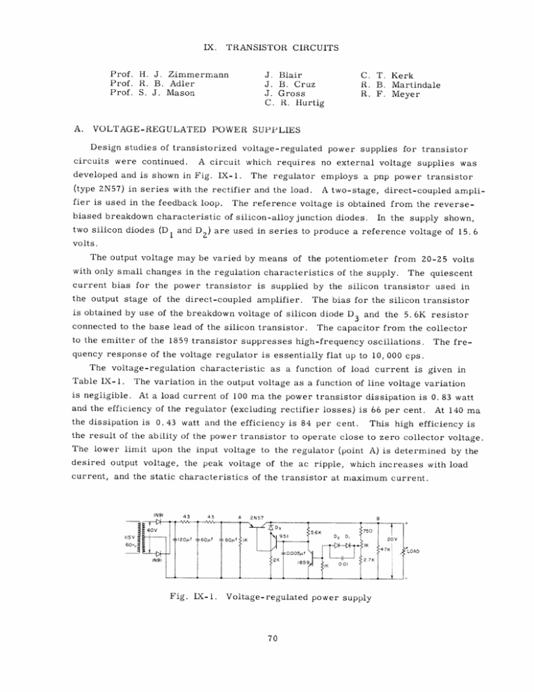
IX. TRANSISTOR CIRCUITS Prof. H. J. Zimmermann Prof. R. B. Adler Prof. S. J. Mason A. VOLTAGE-REGULATED J. Blair J. B. Cruz J. Gross C. R. Hurtig POWER SUPPLIES Design studies of transistorized voltage-regulated circuits were continued. C. T. Kerk R. B. Martindale R. F. Meyer power supplies for transistor A circuit which requires no external voltage supplies was developed and is shown in Fig. IX-1. The regulator employs a pnp power transistor (type 2N57) in series with the rectifier and the load. fier is used in the feedback loop. A two-stage, direct-coupled ampli- The reference voltage is obtained from the reverse- biased breakdown characteristic of silicon-alloy junction diodes. In the supply shown, two silicon diodes (D1 and DZ) are used in series to produce a reference voltage of 15. 6 volts. The output voltage may be varied by means of the potentiometer from 20-25 volts with only small changes in the regulation characteristics of the supply. current bias for the power transistor is The quiescent supplied by the silicon transistor used in the output stage of the direct-coupled amplifier. The bias for the silicon transistor is obtained by use of the breakdown voltage of silicon diode D3 and the 5. 6K resistor connected to the base lead of the silicon transistor. The capacitor from the collector to the emitter of the 1859 transistor suppresses high-frequency oscillations. The fre- quency response of the voltage regulator is essentially flat up to 10, 000 cps. The voltage-regulation characteristic Table IX-1. as a function of load current is given in The variation in the output voltage as a function of line voltage variation is negligible. At a load current of 100 ma the power transistor dissipation is 0. 83 watt and the efficiency of the regulator (excluding rectifier losses) is 66 per cent. At 140 ma the dissipation is 0. 43 watt and the efficiency is 84 per cent. This high efficiency is the result of the ability of the power transistor to operate close to zero collector voltage. The lower limit upon the input voltage to the regulator (point A) is determined by the desired output voltage, the peak voltage of the ac ripple, which increases with load current, and the static characteristics of the transistor at maximum current. IN9 9 .. 43 . 43 A 9K 7 li5V 60-' LOAD Fig. IX-1. Voltage-regulated power supply (IX. TRANSISTOR CIRCUITS) Voltage Regulation Characteristics Table IX-1. Load Current (ma) Direct Voltage (v) Ripple Voltage (v) (peak-to-peak) A B (change from nominal value of 20 v) A B 0 40 0 0.30 <0.001 50 34 -0.02 0.55 <0.001 100 28 -0.05 0.70 <0.001 140 23 -0.08 0.80 0.001 Voltage regulators of this same general configuration having nominal output voltages from 3-25 volts were designed and tested. The lower limit of the output voltage is determined by the availability of silicon diodes with low values of reverse breakdown The upper limit of the output voltage is determined by the maximum voltage voltage. ratings of the transistors. In the circuit shown the maximum load current is limited by the maximum value of the reverse current of the diode D 3 , and the gain of the series transistor. The current in the diode is maximum at no-load and its value is determined by the desired change in load current and the large signal gain of the series transistor over this range. Since the breakdown voltage of the reference diodes has some temperature dependence (the ones used varied by about 0. 08 per cent/°C), the output voltage will have at least an equal temperature dependence. pensation by means of thermistors, employed. To reduce this temperature dependence, com- or by auxiliary forward-biased diodes, may be Alternatively of course, the diodes may be replaced by batteries having low- temperature coefficients. C. T. Kerk B. A MICROSCOPIC INTERPRETATION OF POWER GAIN IN JUNCTION TRANSISTORS In amplifiers of the vacuum-tube variety, it is usually possible to understand the process of power gain by tracing particles and discussing their energy changes as they move. While this procedure is not usually the best way to achieve a quantitative des- cription of the device, it often serves as the root of our qualitative understanding of the gain mechanism. In some cases, it may indeed have been the keystone of the invention of the original device. Peculiarly enough, however, this viewpoint has certainly never been stressed for the transistor, and to the best of our knowledge it has not even been discussed. The following compressed outline presents the major features of an attempt (IX. TRANSISTOR CIRCUITS) to treat the junction transistor through a discussion of the particle energies involved (1). We recognize first that "class A" power gain shows up inside a resistive amplifying device as a change in the internal power dissipation. tion process is therefore required. A microscopic view of the dissipa- We achieve this view by writing an energy balance relation for clouds of holes and free electrons in a semiconductor which is slightly out of thermal equilibrium. In notation which is now standard (2), statistical mechanics leads to the concept of quasi-Fermi levels for holes and free electrons out of equilibrium = p + (kT/q) In (p/n.) 1 (1) - (kT/q) In (n/n S= i) The hole and free electron current densities are then given by P = -q Lp p V p (2) In = -q n V n leading to the notion of generalized nonequilibrium forces F p, n Fp = -q V4p = -q Vi - k V[T In (p/pi)] (3) Fn = +q Vqn = +q VY - k V[T In (n/ni)] which are conservative. The potential energies of the carriers at a point s in the non- equilibrium force field are defined in volts as I (s) = q p F p d9 = p (s) - pmin min (4) s I1n (s) = q Fn di = -[(s)n - nn min in] min where the zero point is taken at the position where of particle. 4 is minimum for each type The organized drift velocities are -p Vdp qp p p (5) Vdn -I qn n Vn (IX. TRANSISTOR CIRCUITS) The assumption of small departures from equilibrium implies that organized transport kinetic energy terms 1/2 m vd are negligible. Therefore the work done by nonequilibrium forces goes into the lattice as "conductive dissipation" P -F d cp dp Pq P pp pl 2 p (6) In Pnp = Vdn Fn qn7 n n 2 inn n If we consider the hole and free electron clouds as open systems, the energy of configuration plus thermal energy of each particle can be shown to be E w p = 3 g 2q /2 kT q (7) w n where E = 3/2 q + 2q is the energy gap, and hole and free electron masses are taken to be equal. Thus the entire energy per particle is E g + 11 Zq p Eg kT pp = 3/2 q kT + n 3/ =3/2 -- + 1 (8) n We now note that the energy of a unit volume of a cloud may change by four processes: 1. recombination of particles, 3. convection of particles, 2. with the lattice (conductive dissipation), and 4. collision of particles change of 0 with time at constant par- The expression of the total energy balance of the clouds per unit ticle concentration. volume then becomes q at (p p) -V. ( p)- qr(np- n p)p + I Vp + qp p 0)n n) - qr(np - n (In q a (n n Vn n + qn (9) at at If Eqs. 9 are expanded fully, they become nothing but the continuity equations for the flow of holes and free electrons. -- q p at ( - ) p p Expanding only the left side, however, qr( qr(np- L - np yields PVp 0 (10) q n =v. ( n) - [qr(np - noPo) n + n V n] (IX. TRANSISTOR CIRCUITS) The term in brackets, as we have seen, is the total dissipation per unit volume, and the divergence term represents convection of energy into the volume. Thus the left sides are interpreted as the rate of increase of stored (recoverable) energy per unit volume. If we treat the temperature T and the gap E nonequilibrium potentials HI, on, we may write Eqs. p n = = ' +I p ' + as variables independent of the g since the latter can be altered by light, voltage, and so 8 as p (11) 1n Because the energy balance relations (Eq. 10) are linear in separated into two sets, one in p and n ' and one in II, for each particle type. they can then be The equations involving IH have been checked for dissipation in an idealized transistor under quiescent conditions, and as a low-frequency amplifier. In both cases the dissipation checks with computations from the equivalent circuit. More work remains to be done on the fully time-varying case, and in connection with the equations involving only }'. R. B. Adler for J. Blair References 1. See J. Blair, Theory of power gain in junction transistors, S. M. Thesis, Department of Electrical Engineering, M. I. T., Sept. 1, 1955, for further details. 2. W. Shockley, Electrons and Holes in Semiconductors (D. Van Nostrand Company, Inc., New York, 1950).


