Pin Assignment for Multi-FPGA Systems (Extended Abstract)
advertisement

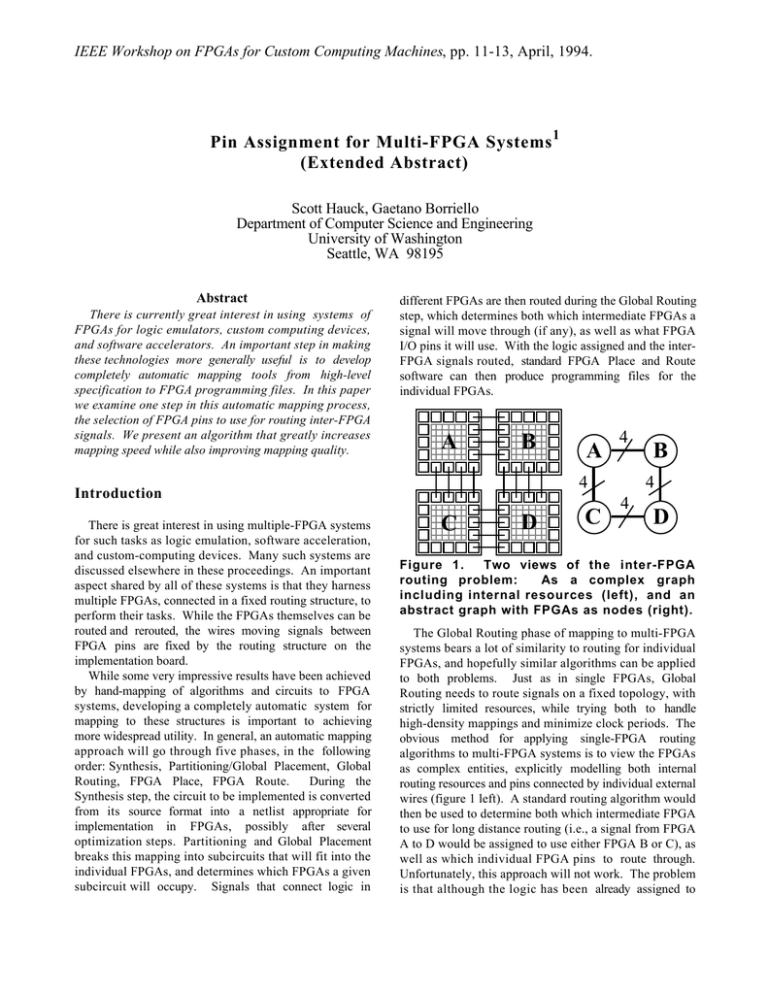
IEEE Workshop on FPGAs for Custom Computing Machines, pp. 11-13, April, 1994. Pin Assignment for Multi-FPGA Systems 1 (Extended Abstract) Scott Hauck, Gaetano Borriello Department of Computer Science and Engineering University of Washington Seattle, WA 98195 Abstract There is currently great interest in using systems of FPGAs for logic emulators, custom computing devices, and software accelerators. An important step in making these technologies more generally useful is to develop completely automatic mapping tools from high-level specification to FPGA programming files. In this paper we examine one step in this automatic mapping process, the selection of FPGA pins to use for routing inter-FPGA signals. We present an algorithm that greatly increases mapping speed while also improving mapping quality. different FPGAs are then routed during the Global Routing step, which determines both which intermediate FPGAs a signal will move through (if any), as well as what FPGA I/O pins it will use. With the logic assigned and the interFPGA signals routed, standard FPGA Place and Route software can then produce programming files for the individual FPGAs. A B 4 4 Introduction There is great interest in using multiple-FPGA systems for such tasks as logic emulation, software acceleration, and custom-computing devices. Many such systems are discussed elsewhere in these proceedings. An important aspect shared by all of these systems is that they harness multiple FPGAs, connected in a fixed routing structure, to perform their tasks. While the FPGAs themselves can be routed and rerouted, the wires moving signals between FPGA pins are fixed by the routing structure on the implementation board. While some very impressive results have been achieved by hand-mapping of algorithms and circuits to FPGA systems, developing a completely automatic system for mapping to these structures is important to achieving more widespread utility. In general, an automatic mapping approach will go through five phases, in the following order: Synthesis, Partitioning/Global Placement, Global Routing, FPGA Place, FPGA Route. During the Synthesis step, the circuit to be implemented is converted from its source format into a netlist appropriate for implementation in FPGAs, possibly after several optimization steps. Partitioning and Global Placement breaks this mapping into subcircuits that will fit into the individual FPGAs, and determines which FPGAs a given subcircuit will occupy. Signals that connect logic in A C D C B 4 4 D Figure 1. Two views of the inter-FPGA routing problem: As a complex graph including internal resources (left), and an abstract graph with FPGAs as nodes (right). The Global Routing phase of mapping to multi-FPGA systems bears a lot of similarity to routing for individual FPGAs, and hopefully similar algorithms can be applied to both problems. Just as in single FPGAs, Global Routing needs to route signals on a fixed topology, with strictly limited resources, while trying both to handle high-density mappings and minimize clock periods. The obvious method for applying single-FPGA routing algorithms to multi-FPGA systems is to view the FPGAs as complex entities, explicitly modelling both internal routing resources and pins connected by individual external wires (figure 1 left). A standard routing algorithm would then be used to determine both which intermediate FPGA to use for long distance routing (i.e., a signal from FPGA A to D would be assigned to use either FPGA B or C), as well as which individual FPGA pins to route through. Unfortunately, this approach will not work. The problem is that although the logic has been already assigned to FPGAs during partitioning, the placement of logic into individual logic blocks will not be done until the next step, FPGA placement. Thus, since there is no specific source or sink for the individual routes, standard routing algorithms cannot be applied. The approach we take here is to abstract entire FPGAs into single nodes in the routing graph, with the arcs between the nodes representing bundles of wires. This solves the unassigned source and sink problem mentioned above, since while the logic hasn’t been placed into individual logic blocks, partitioning has assigned the logic to the FPGAs. It also simplifies the routing problem, since the graph is much simpler, and similar resources are grouped together (i.e. all wires connecting the same FPGAs are grouped together into a single edge in the graph). Unfortunately, the routing algorithm can no longer determine the individual FPGA pins a signal should use, since those details have been abstracted away. It is this problem, the assignment of interchip routing signals to FPGA I/O pins, that the rest of this paper addresses. Pin assignment for multi-FPGA systems One solution to the pin assignment problem is quite simple: ignore it. After Global Routing has routed signals through intermediate FPGAs, those signals are then randomly assigned to individual pins. While this simple approach can quickly generate an assignment, it gives up some optimization opportunities. A poor pin assignment can not only result in greater delay and lower logic density, but can also slow down the place and route software, which must deal with a more complex mapping problem. A second solution is to use a topology that simplifies the problem. Specifically, topologies such as bipartite graphs only connect logic-bearing FPGAs with routingonly FPGAs. In this way, the logic-bearing FPGAs can be placed initially, and it is assumed that the routing-only FPGAs can handle any possible pin assignment. More details on such an approach can be found in [1]. However, it is important to note that these approaches only apply to topologies such as bipartite graphs and partial crossbars, topologies where logic-bearing FPGAs are not directly connected. A third approach is to allow the FPGA placement tool to determine its own assignment. This requires that the placement tool allow the user to restrict the locations where an I/O pin can be assigned (e.g., Xilinx APR and PPR placement and routing tools [4]). With such a system, I/O signals are restricted to only those pin locations that are wired to the proper destinations. Once the placement tool determines the pin assignment for one FPGA, this assignment is propagated to the attached FPGAs. It is important to note that this does limit the number of placement runs that can be performed in parallel. Specifically, since the assignment from one FPGA is propagated to adjacent FPGAs only after that entire FPGA has been placed, no two adjacent FPGAs can be placed simultaneously. Since the placement and routing steps can be the most time-consuming steps in the mapping process, achieving the greatest parallelism in this task can be critical. Also, while the iterative placement approach can optimize locally, creating good results in a single FPGA, it ignores more global optimization opportunities. Finally, there are some topologies for which iterative placement may be unable to determine a correct pin assignment, because the placement of one FPGA may use up resources required in another FPGA. Force-directed pin assignment for multiFPGA systems As we have discussed, pin assignment via sequential placement of individual FPGAs can be slow, cannot optimize globally, and may not work at all for some topologies. What is necessary is a more global approach which optimizes the entire mapping, while avoiding sequentializing the placement step. Intuitively, the best approach to pin assignment would be to simultaneously place all FPGAs, with the individual placement runs communicating with each other to balance the pin assignment demands of each FPGA. In this way a global optimum could be reached, and the mapping of all FPGAs would be completed as quickly as any single placement could be accomplished. Unfortunately, tools to do this do not exist, and the communication necessary to perform this task could become prohibitive. Our approach is similar to simultaneous placement, but we will perform the assignment on a single machine within a single process. Obviously, with the placement of a single FPGA consuming considerable CPU time, complete placement of all FPGAs simultaneously on a single processor is impractical, and thus simplification of the problem will be key to a workable solution. Our approach is to use force-directed placement of the individual FPGAs [3]. In force-directed placement, the signals that connect logic in a mapping are replaced by springs between the signal’s source and each sink, and the placement process consists of seeking a minimum net force placement of the logic. By finding this minimum net force configuration, we expect to minimize wirelength in the resulting mapping. To find this configuration, the software randomly chooses a logic block and moves it to its minimum net force location. This hill-climbing process continues until a local optimum is found, at which point the software accepts the current configuration. Force-directed placement may seem a poor choice for pin assignment, and is generally felt to be inferior to simulated annealing for FPGA placement. Two reasons for this are the difficulty force-directed placement has with optimizing for goals other than wirelength, and the inaccuracy of the spring approximation to routing costs. However, force-directed placement can handle all of the optimization tasks involved in pin assignment, and the spring metric is the key to efficient handling of multiFPGA systems. 1 A B U 2 3 (2*3) (2+3+5) 5 A C A B (2*5) (2+3+5) 1.6 1.0 B 1 1.5 (3*5) (2+3+5) C C Figure 2. Example of spring simplification rules. Source circuit at top has node U replaced at middle, and any springs created in parallel to others are merged at bottom. As implied earlier, we will not simply place individual FPGAs, but will in fact use force-directed placement simultaneously on all FPGAs in the system. To make this tractable, we can simplify the mapping process. Specifically, since we are only performing pin assignment, we do not care where the individual logic blocks are placed. Thus, we can examine the system of springs built for the circuit mapping, and use the laws of physics to remove nodes corresponding to FPGA logic blocks, leaving only 1 This paper is an extended abstract of University of Washington, Dept. of Computer Science & Engineering Technical Report #94-04-01, April 1994. I/O pins. As shown in the example of figure 5, the springs connected between an internal logic node and its neighbors can be replaced with a set of springs connected between the node’s neighbors while maintaining the exact same forces on the other nodes. By repeatedly applying these simplification rules to the logic nodes in the system, we end up with a mapping consisting only of I/O pins, with spring connections that act identically to the complete mapping they replace. In this way, we simplify the problem enough to allow the pin assignment of a large system of FPGAs to be performed efficiently. We have performed comparisons of our force-directed approach with iterative placement approaches, as well as random pin assignments, on several current multi-FPGA systems. The results have shown that the force directed approach is faster than all other alternatives, including random, by up to almost a factor of ten. It also produces higher-quality results than the other approaches, yielding up to an 8.5% decrease in total wirelength in the system. Our algorithm works on arbitrary topologies, including those for which iterative placement approaches generate incorrect results. Complete results, along with a more thorough discussion of this topic, can be found in [2]. References [1] P. K. Chan, M. D. F. Schlag, "Architectural Tradeoffs in Field-Programmable-Device-Based Computing Systems", IEEE Workshop on FPGAs for Custom Computing Machines, pp. 152-161, 1993. [2] S. Hauck, G. Borriello, "Pin Assignment for Multi-FPGA Systems", University of Washington, Dept. of Computer Science & Engineering Technical Report #94-04-01, April 1994. [3] K. Shahookar, P. Mazumder, “VLSI Cell Placement Techniques”, ACM Computing Surveys, Vol. 23, No. 2, pp. 145-220, June 1991. [4] Xilinx Development System Reference Guide and The Programmable Logic Data Book, Xilinx, Inc., San Jose, CA, 1993.


