Microcontact Printing (µCP) 1 Transfer master casting
advertisement
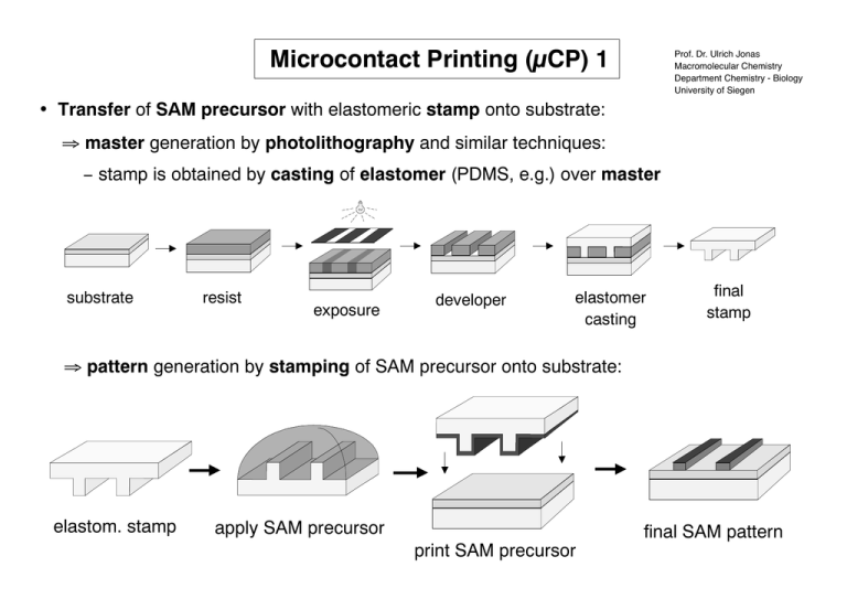
Microcontact Printing (µCP) 1 Prof. Dr. Ulrich Jonas Macromolecular Chemistry Department Chemistry - Biology University of Siegen Transfer of SAM precursor with elastomeric stamp onto substrate: master generation by photolithography and similar techniques: stamp is obtained by casting of elastomer (PDMS, e.g.) over master substrate resist exposure developer elastomer casting final stamp pattern generation by stamping of SAM precursor onto substrate: elastom. stamp apply SAM precursor print SAM precursor final SAM pattern Microcontact Printing (µCP) 2 Stamped SAM pattern can be further processed by etching or deposition: µCP technique can also be applied to curved surfaces of stamp or substrate curved stamp curved substrate etching deposition quality of µCP SAMs is comparable to films obtained by adsorption from solution stamp stamp solution stamp solution solution Replica Molding (REM) Use elastic stamp as master for molding of rigid polymer: elasticity and low surface energy of stamp make release of mold easy Microtransfer Molding (µTM) convenient method for fabrication of microstructures on nonplanar substrates and 3D structures layer by layer: Micromolding in Capillaries (MIMIC) 3D microstructure formation by filling of microcapillaries with liquid precursor: polymer precursor: A, C: polyacrylate B, D: polyurethane precursor w/ solvent: A, B: polymer beads C, D: polyaniline emeraldine · HCl Solvent Assisted Micromolding (SAMIM) Quasi 3D microstructure formation in polymeric substrates by solvent etching in microcapillaries: polymer film: photoresist, solvent: ethanol Proximal Probe Lithography / Scanning Probe Lithography Use of scanning probe microscopes for surface modification down to the nm range: electrical methods: scanning tunneling microscope (STM) tip generates local field / current which modifies region under tip (SiH Si) mechanical methods: scanning force microscope (SFM / AFM) tip scrapes or transfers material at the surface optical methods: near field optical scanning microscope (NSOM) tip exposes photoresist under tip Embossing Rigid master (stamp, Ni or SiO2, e.g.) is pressed into thermally softened polymer substrate (PMMA, polycarbonate CD, e.g.) to transfer relief structure to polymer: 1. Press mold 2. Remove mold application: microchip for isotachophoresis (electrophoretic separation technique for ionic compounds) 3. Etching Microcutting: embossing of metal coated polymer films creates metallic micro objects application: IR polarizer, polarization dependent color filter (on the right) Printing (Inkjet) Inkjet printer can be used to generate surface pattern with appropriate "ink" (resolution ~50 µm): resist: by using a resist precursor as ink the mask can be printed directly electr. active materials: "printing" of electronic devices, like thin film transistors (TFT) DNA: generate DNA arrays for sequencing applications polymers: printing of polymer precursors for rapid 3D prototyping (layer by layer) TFT printing: microlense printing:
