Application Note AN-3005 Design Fundamentals for Phototransistor Circuits www.fairchildsemi.com
advertisement
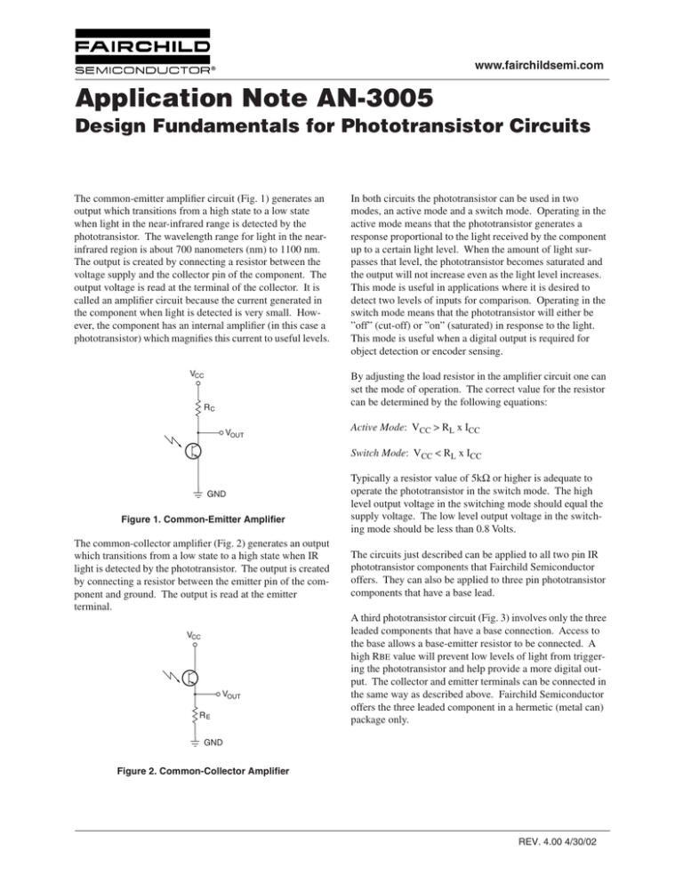
www.fairchildsemi.com Application Note AN-3005 Design Fundamentals for Phototransistor Circuits The common-emitter amplifier circuit (Fig. 1) generates an output which transitions from a high state to a low state when light in the near-infrared range is detected by the phototransistor. The wavelength range for light in the nearinfrared region is about 700 nanometers (nm) to 1100 nm. The output is created by connecting a resistor between the voltage supply and the collector pin of the component. The output voltage is read at the terminal of the collector. It is called an amplifier circuit because the current generated in the component when light is detected is very small. However, the component has an internal amplifier (in this case a phototransistor) which magnifies this current to useful levels. VCC In both circuits the phototransistor can be used in two modes, an active mode and a switch mode. Operating in the active mode means that the phototransistor generates a response proportional to the light received by the component up to a certain light level. When the amount of light surpasses that level, the phototransistor becomes saturated and the output will not increase even as the light level increases. This mode is useful in applications where it is desired to detect two levels of inputs for comparison. Operating in the switch mode means that the phototransistor will either be ”off” (cut-off) or ”on” (saturated) in response to the light. This mode is useful when a digital output is required for object detection or encoder sensing. By adjusting the load resistor in the amplifier circuit one can set the mode of operation. The correct value for the resistor can be determined by the following equations: RC VOUT Active Mode: VCC > RL x ICC Switch Mode: VCC < RL x ICC GND Figure 1. Common-Emitter Amplifier The common-collector amplifier (Fig. 2) generates an output which transitions from a low state to a high state when IR light is detected by the phototransistor. The output is created by connecting a resistor between the emitter pin of the component and ground. The output is read at the emitter terminal. VCC VOUT RE Typically a resistor value of 5kΩ or higher is adequate to operate the phototransistor in the switch mode. The high level output voltage in the switching mode should equal the supply voltage. The low level output voltage in the switching mode should be less than 0.8 Volts. The circuits just described can be applied to all two pin IR phototransistor components that Fairchild Semiconductor offers. They can also be applied to three pin phototransistor components that have a base lead. A third phototransistor circuit (Fig. 3) involves only the three leaded components that have a base connection. Access to the base allows a base-emitter resistor to be connected. A high RBE value will prevent low levels of light from triggering the phototransistor and help provide a more digital output. The collector and emitter terminals can be connected in the same way as described above. Fairchild Semiconductor offers the three leaded component in a hermetic (metal can) package only. GND Figure 2. Common-Collector Amplifier REV. 4.00 4/30/02 AN-3005 APPLICATION NOTE Finally, the phototransistor should be biased (voltage applied to VCC) with 5 Volts. The maximum bias is 16 V, however the performance of the component doesn’t change with a greater bias except when the phototransistor is used as a switch -- the high level output will equal the higher setting. VCC RC VOUT R BE GND GND Note: Fairchild’s photodarlington products can be used in the same manner as the phototransistors. The photodarlingtons will provide greater outputs for the same light level because they have a greater internal gain, but will have a higher saturation voltage and slower turnoff than the phototransistor devices. Figure 3. Phototransistor Circuit with Base Connection DISCLAIMER FAIRCHILD SEMICONDUCTOR RESERVES THE RIGHT TO MAKE CHANGES WITHOUT FURTHER NOTICE TO ANY PRODUCTS HEREIN TO IMPROVE RELIABILITY, FUNCTION OR DESIGN. FAIRCHILD DOES NOT ASSUME ANY LIABILITY ARISING OUT OF THE APPLICATION OR USE OF ANY PRODUCT OR CIRCUIT DESCRIBED HEREIN; NEITHER DOES IT CONVEY ANY LICENSE UNDER ITS PATENT RIGHTS, NOR THE RIGHTS OF OTHERS. LIFE SUPPORT POLICY FAIRCHILD’S PRODUCTS ARE NOT AUTHORIZED FOR USE AS CRITICAL COMPONENTS IN LIFE SUPPORT DEVICES OR SYSTEMS WITHOUT THE EXPRESS WRITTEN APPROVAL OF THE PRESIDENT OF FAIRCHILD SEMICONDUCTOR CORPORATION. As used herein: 1. Life support devices or systems are devices or systems which, (a) are intended for surgical implant into the body, or (b) support or sustain life, or (c) whose failure to perform when properly used in accordance with instructions for use provided in the labeling, can be reasonably expected to result in significant injury to the user. 2. A critical component is any component of a life support device or system whose failure to perform can be reasonably expected to cause the failure of the life support device or system, or to affect its safety or effectiveness. www.fairchildsemi.com 4/30/02 0.0m 001 Stock#AN300000xx 2002 Fairchild Semiconductor Corporation
