Document 10494985
letters to nature
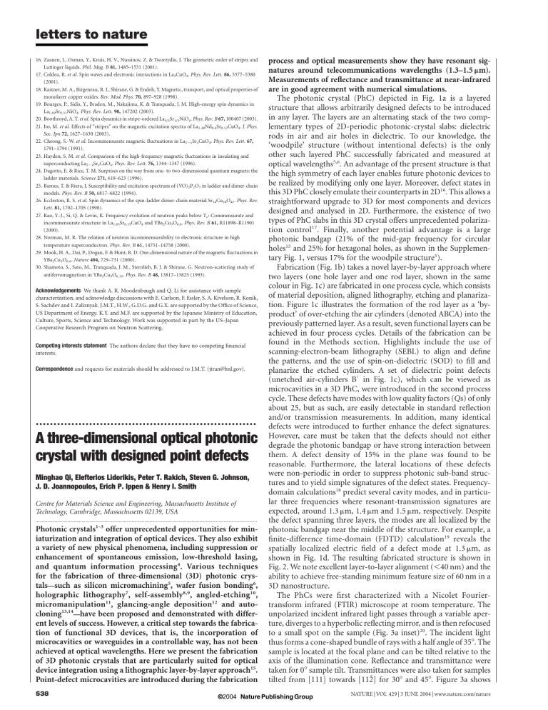
16. Zaanen, J., Osman, Y., Kruis, H. V., Nussinov, Z. & Tworzydlo, J. The geometric order of stripes and
Luttinger liquids.
Phil. Mag. B 81, 1485–1531 (2001).
17. Coldea, R.
et al.
Spin waves and electronic interactions in La
2
CuO
4
.
Phys. Rev. Lett.
86, 5377–5380
(2001).
18. Kastner, M. A., Birgeneau, R. J., Shirane, G. & Endoh, Y. Magnetic, transport, and optical properties of monolayer copper oxides.
Rev. Mod. Phys.
70, 897–928 (1998).
19. Bourges, P., Sidis, Y., Braden, M., Nakajima, K. & Tranquada, J. M. High-energy spin dynamics in
La
1.69
Sr
0.31
NiO
4
.
Phys. Rev. Lett.
90, 147202 (2003).
20. Boothroyd, A. T.
et al.
Spin dynamics in stripe-ordered La
5/3
Sr
1/3
NiO
4
.
Phys. Rev. B 67, 100407 (2003).
21. Ito, M.
et al.
Effects of “stripes” on the magnetic excitation spectra of La
1.48
Nd
0.4
Sr
0.12
CuO
4
.
J. Phys.
Soc. Jpn 72, 1627–1630 (2003).
22. Cheong, S.-W.
et al.
Incommensurate magnetic fluctuations in La
2 2 x
Sr x
CuO
4
.
Phys. Rev. Lett.
67,
1791–1794 (1991).
23. Hayden, S. M.
et al.
Comparison of the high-frequency magnetic fluctuations in insulating and superconducting La
2 2 x
Sr x
CuO
4
.
Phys. Rev. Lett.
76, 1344–1347 (1996).
24. Dagotto, E. & Rice, T. M. Surprises on the way from one- to two-dimensional quantum magnets: the ladder materials.
Science 271, 618–623 (1996).
25. Barnes, T. & Riera, J. Susceptibility and excitation spectrum of (VO)
2
P
2
O
7 in ladder and dimer-chain models.
Phys. Rev. B 50, 6817–6822 (1994).
26. Eccleston, R. S.
et al.
Spin dynamics of the spin-ladder dimer-chain material Sr
14
Cu
24
O
41
.
Phys. Rev.
Lett.
81, 1702–1705 (1998).
27. Kao, Y.-J., Si, Q. & Levin, K. Frequency evolution of neutron peaks below T c
: Commensurate and incommensurate structure in La
1.85
Sr
0.15
CuO
4 and YBa
2
Cu
3
O
6.6
.
Phys. Rev. B 61, R11898–R11901
(2000).
28. Norman, M. R. The relation of neutron incommensurability to electronic structure in high temperature superconductors.
Phys. Rev. B 61, 14751–14758 (2000).
29. Mook, H. A., Dai, P., Dogan, F. & Hunt, R. D. One-dimensional nature of the magnetic fluctuations in
YBa
2
Cu
3
O
6.6
.
Nature 404, 729–731 (2000).
30. Shamoto, S., Sato, M., Tranquada, J. M., Sternlieb, B. J. & Shirane, G. Neutron-scattering study of antiferromagnetism in YBa
2
Cu
3
O
6.15
.
Phys. Rev. B 48, 13817–13825 (1993).
Acknowledgements We thank A. R. Moodenbaugh and Q. Li for assistance with sample characterization, and acknowledge discussions with E. Carlson, F. Essler, S. A. Kivelson, R. Konik,
S. Sachdev and I. Zaliznyak. J.M.T., H.W., G.D.G. and G.X. are supported by the Office of Science,
US Department of Energy. K.Y. and M.F. are supported by the Japanese Ministry of Education,
Culture, Sports, Science and Technology. Work was supported in part by the US–Japan
Cooperative Research Program on Neutron Scattering.
Competing interests statement The authors declare that they have no competing financial interests.
Correspondence and requests for materials should be addressed to J.M.T. (jtran@bnl.gov).
..............................................................
A three-dimensional optical photonic crystal with designed point defects
Minghao Qi, Elefterios Lidorikis, Peter T. Rakich, Steven G. Johnson,
J. D. Joannopoulos, Erich P. Ippen & Henry I. Smith
Centre for Materials Science and Engineering, Massachusetts Institute of
Technology, Cambridge, Massachusetts 02139, USA
.............................................................................................................................................................................
Photonic crystals 1–3 offer unprecedented opportunities for miniaturization and integration of optical devices. They also exhibit a variety of new physical phenomena, including suppression or enhancement of spontaneous emission, low-threshold lasing, and quantum information processing 4 . Various techniques for the fabrication of three-dimensional (3D) photonic crystals—such as silicon micromachining 5 holographic lithography 7
, wafer fusion bonding
, self-assembly 8,9 , angled-etching
6
10 ,
, micromanipulation 11 , glancing-angle deposition 12 and autocloning 13,14 —have been proposed and demonstrated with different levels of success. However, a critical step towards the fabrication of functional 3D devices, that is, the incorporation of microcavities or waveguides in a controllable way, has not been achieved at optical wavelengths. Here we present the fabrication of 3D photonic crystals that are particularly suited for optical device integration using a lithographic layer-by-layer approach 15 .
Point-defect microcavities are introduced during the fabrication
538
© 200 4 Nature Publishing Group process and optical measurements show they have resonant signatures around telecommunications wavelengths (1.3–1.5
m m).
Measurements of reflectance and transmittance at near-infrared are in good agreement with numerical simulations.
The photonic crystal (PhC) depicted in Fig. 1a is a layered structure that allows arbitrarily designed defects to be introduced in any layer. The layers are an alternating stack of the two complementary types of 2D-periodic photonic-crystal slabs: dielectric rods in air and air holes in dielectric. To our knowledge, the
‘woodpile’ structure (without intentional defects) is the only other such layered PhC successfully fabricated and measured at optical wavelengths 5,6 . An advantage of the present structure is that the high symmetry of each layer enables future photonic devices to be realized by modifying only one layer. Moreover, defect states in this 3D PhC closely emulate their counterparts in 2D 16 . This allows a straightforward upgrade to 3D for most components and devices designed and analysed in 2D. Furthermore, the existence of two types of PhC slabs in this 3D crystal offers unprecedented polarization control 17 . Finally, another potential advantage is a large photonic bandgap (21% of the mid-gap frequency for circular holes 15 and 25% for hexagonal holes, as shown in the Supplementary Fig. 1, versus 17% for the woodpile structure 5 ).
Fabrication (Fig. 1b) takes a novel layer-by-layer approach where two layers (one hole layer and one rod layer, shown in the same colour in Fig. 1c) are fabricated in one process cycle, which consists of material deposition, aligned lithography, etching and planarization. Figure 1c illustrates the formation of the rod layer as a ‘byproduct’ of over-etching the air cylinders (denoted ABCA) into the previously patterned layer. As a result, seven functional layers can be achieved in four process cycles. Details of the fabrication can be found in the Methods section. Highlights include the use of scanning-electron-beam lithography (SEBL) to align and define the patterns, and the use of spin-on-dielectric (SOD) to fill and planarize the etched cylinders. A set of dielectric point defects
0
(unetched air-cylinders B in Fig. 1c), which can be viewed as microcavities in a 3D PhC, were introduced in the second process cycle. These defects have modes with low quality factors ( Q s) of only about 25, but as such, are easily detectable in standard reflection and/or transmission measurements. In addition, many identical defects were introduced to further enhance the defect signatures.
However, care must be taken that the defects should not either degrade the photonic bandgap or have strong interaction between them. A defect density of 15% in the plane was found to be reasonable. Furthermore, the lateral locations of these defects were non-periodic in order to suppress photonic sub-band structures and to yield simple signatures of the defect states. Frequencydomain calculations 18 predict several cavity modes, and in particular three frequencies where resonant-transmission signatures are expected, around 1.3
m m, 1.4
m m and 1.5
m m, respectively. Despite the defect spanning three layers, the modes are all localized by the photonic bandgap near the middle of the structure. For example, a finite-difference time-domain (FDTD) calculation 19 reveals the spatially localized electric field of a defect mode at 1.3
m m, as shown in Fig. 1d. The resulting fabricated structure is shown in
Fig. 2. We note excellent layer-to-layer alignment ( , 40 nm) and the ability to achieve free-standing minimum feature size of 60 nm in a
3D nanostructure.
The PhCs were first characterized with a Nicolet Fouriertransform infrared (FTIR) microscope at room temperature. The unpolarized incident infrared light passes through a variable aperture, diverges to a hyperbolic reflecting mirror, and is then refocused to a small spot on the sample (Fig. 3a inset) 20 . The incident light thus forms a cone-shaped bundle of rays with a half angle of 35 8 . The sample is located at the focal plane and can be tilted relative to the axis of the illumination cone. Reflectance and transmittance were taken for 0 8 sample tilt. Transmittances were also taken for samples tilted from [111] towards [112¯] for 30 8 and 45 8 . Figure 3a shows
NATURE | VOL 429 | 3 JUNE 2004 | www.nature.com/nature
letters to nature some typical transmission and reflection spectra. A stop-band is observed from 1.15
m m to 1.6
m m for all tilt angles. It is important to note that for non-zero sample tilt angles, each recorded spectrum is actually an average over a variety of incident angles. For example, a transmission spectrum at 45 8 sample tilt includes incident angles from 10 8 to 80 8 . Therefore these measurements clearly demonstrate an omni-directional photonic bandgap. Quantitatively, the reflectance and transmittance in the 0 8 sample tilt (corresponding to a small range of incident angles around 35 8 with respect to the sample normal) add up to (100 ^ 6)% for a wide wavelength range from
1.31
m m up to 2.45
m m. Furthermore, the transmission and reflection curves cross at 1.68
m m with exactly 50% transmission and 50% reflection. At short wavelengths, in the vicinity of the upper edge of the bandgap, reflectance drops down as theory predicts. The fact that an associated transmittance increase is not observed is most likely due to the fact that we were near the measurement noise floor of the spectrometer at those wavelengths. A stronger light source, as we shall describe shortly, indeed yielded high transmittance at short wavelengths. If we define the threshold as where transmittance is less than 25% and reflectance is more than 75%, the bandgap extends from 1.15
m m to 1.45
m m, corresponding to 23% of the mid-gap frequency. This verifies the large 3D bandgap of our structure and is in good agreement with the theoretical prediction of 21% full bandgap 15 .
A pronounced defect signature can be clearly seen at 1.3
m m, in the middle of the 3D bandgap, as a dip in the reflection and corresponding increase in transmission (Fig. 3a). In a control experiment, a previously fabricated structure without defects did not show such a dip in the bandgap. Moreover, the independence of resonant frequencies on excitation angle is strong evidence for the microcavity states. To our knowledge, this is the first direct experimental observation of microcavity states in a 3D PhC at optical wavelengths.
To understand the defect states quantitatively, the measured feature sizes (using a scanning-electron microscope whose stage motion is monitored by a laser interferometer) of a fabricated 3D
PhC were fed into an FDTD simulator to calculate the reflection spectrum for a 35 8 incident angle. The simulation is detailed in the
Methods section. A comparison of measured and calculated spectra is shown in Fig. 3b, with good agreement. Although this level of agreement has not been reported in any previous work, a more critical comparison reveals that the defect resonance at 1.3
m m appears somewhat broader than expected. This can be accounted for by inhomogeneous broadening, as the measurements were averaged over many individual point-defects. Small structural variation of individual defects is unavoidable given the limitations of current nanofabrication. In addition, the finer signatures of the defect modes shown in the simulation, including those near 1.4
and 1.5
m m, are not discernable in the measurement.
m m
The above-mentioned issues were resolved with spatially localized measurements of transmission and reflection, which were performed with an ultra-bright, broadband (1.1
m m to 1.9
m m), unpolarized white light produced through supercontinuum generation 21 . A lensed optical-fibre was used to focus the light to a spot of
2.5
m m diameter. For a defect density of 15%, a 2.5m m spot would, on average, sample three defects. This significantly reduces the degree of inhomogeneous broadening for the defect resonances, allowing us to observe the spectral characteristics of individual defect states, which was not possible with the FTIR microscope.
A comparison of measurement and simulation for transmittance is shown in Fig. 4a. The resonance at 1.3
m m demonstrates remarkable agreement between measurement and simulation in terms of resonance magnitude and line-width. The Q of this defect mode is found to be approximately 25 from simulation, which assumes no inhomogeneous broadening, whereas the measurement achieves a
Q of approximately 18. Simulation also proves that this resonance peak does correspond to a localized defect state in the 3D PhC. The field pattern within the PhC, excited by a planewave at the resonance frequency of 1.3
m m, was calculated and is shown in Fig. 1d, which exhibits strong field localization at the defect. In addition, a new
Figure 1 Schematic of the 3D PhC and its fabrication in silicon (Si).
a , Computer rendering of an ideal 3D PhC with three hole layers and three rod layers. The fabricated structure has one additional hole layer on top of the uppermost rod layer.
b , An illustration of the layer-by-layer approach, showing two process cycles and the over-etch into the previous layer. Details of the process flow can be found in the Methods section.
NATURE | VOL 429 | 3 JUNE 2004 | www.nature.com/nature c , Cross-sectional view in the [11¯0] plane. The PhC can be viewed as a face-centredcubic lattice of air cylinders (denoted ABCA) in high dielectric (Si). Unetched air cylinders, denoted by B
0
, form ‘dielectric’ point defects.
d , Calculated e j E j 2
(where e is the dielectric constant, and E is the electric field) of the point-defect state at a resonant wavelength of
1.3
m m. Note, localization of the electric field near the middle of the crystal region.
© 200 4 Nature Publishing Group
539
letters to nature resonance peak near 1.5
m m, which was predicted by theory but not apparent in FTIR measurement, can now be identified in the measurement and is in good agreement with simulation.
The supercontinuum measurement at normal incidence is consistent with the FTIR measurement: it has similar attenuation in transmission but a wider bandgap, as expected from theory. Moreover, at short wavelengths, the transmittance does rebound. A comparison with the perfect 3D PhC without defects, whose transmission response was calculated and is shown as a dashed green line in Fig. 4a, is also noteworthy: the position and size of the bandgap does not change appreciably, indicating that the introduction of defects does not degrade the photonic bandgap.
A comparison of measurement and simulation for reflectance is shown in Fig. 4b. The FDTD simulation was performed for an isolated defect using the supercell approximation (that is, a widely separated, very weakly interacting array of point defects).
Remarkable agreement of the resonance frequencies is found in simulation and measurement, which are manifested as dips in the reflection spectrum at wavelengths around 1.3
m m, 1.4
m m and
1.5
m m. In particular, the weak resonance at 1.4
m m—which is predicted by theory but not identified in Figs 3 and 4a—is clearly seen and agrees very well with simulation. Quantitatively, a maximum reflectance of 85% is in reasonable agreement with the FTIR value of 90%. This lower reflectance, compared with both FTIR and simulation, is explained in part by difficulties in measuring absolute reflectivity due to the limited collection angle of the fibre lens, and also position sensitivity of the confocal arrangement.
All the agreements between simulations and measurements, for
Figure 2 Scanning-electron micrographs of the fabricated 3D PhCs.
a , Lowmagnification top view.
b , A close-up showing the hexagonal array of holes, denoted by A, and B and C are the sets of holes underneath the top layer, showing a sequential shift in the horizontal direction. The rod layers are completely blocked by the hole layers.
c , A tilted top view reveals the rod layer.
d , A cross-sectional view. The functional layers are marked by numbers, and the etched air cylinders are outlined with rectangles. The crystal shown here was fabricated in an early batch and exhibits higher surface roughness as well as more deviations from the designed parameters. It was not included for optical characterization.
540
Figure 3 FTIR-microscopy characterization of the 3D PhC with point defects.
broadening.
© 200 4 Nature Publishing Group a , Reflection
(blue, at 0 8 sample tilt) and transmission (red, purple and green, for respective sample tilt angles of 0 8 , 30 8 and 45 8 ). Inset is the optical path of the FTIR microscope. For non-zero degree sample tilts, the spectrum is an average of a variety of incident angles.
b , Comparison of measurement (red) and simulation (blue) for reflection at 35 8 incident angle. No empirical adjustments of any kind were made other than the measured feature sizes. The wider linewidth of the measured defect state is attributed to inhomogeneous
NATURE | VOL 429 | 3 JUNE 2004 | www.nature.com/nature
letters to nature both FTIR and the supercontinuum light source, are particularly noteworthy as no empirical adjustments of any kind (for example, fitting, shifting or rescaling of the spectra) were made either to theory or experiment. The only input into the simulation was the set of measured feature sizes.
Although the agreements of theory and experiment demonstrate the high quality of the fabricated PhC, fabrication imperfections such as surface roughness and misalignment were unavoidable, and indeed showed up in the characterization. At the upper part of the bandgap (wavelengths around 1.2
m m), the photonic crystal appears to produce some loss (that is, reflectance plus transmittance is less than one for both FTIR and supercontinuum measurements). This is expected, as at length scales comparable to the incident wavelength, scattering loss due to surface roughness becomes more significant. The size of the bandgap, when characterized with the supercontinuum source, showed narrowing at places where the fabrication was known to be inferior, such as at the edge or corner of a die.
Finally, we note that the bandgap positions are quite sensitive to the dimensions of the fabricated structures. With the flexibility of electron-beam lithography, we investigated the tuning of bandgaps with structural variations. Specifically, 3D PhCs with the same lattice constant but different hole sizes, corresponding to different filling ratios, were fabricated and measured. The results confirmed the theoretical prediction that a lower Si-filling-ratio results in a shift of the bandgap towards shorter wavelengths.
One important discriminating feature of the lithographic approach used in this work is the ability to fabricate a 3D PhC with intentional defects in a natural, relatively low-cost and flexible manner. More generally, our fabrication process can be applied to a variety of 3D nanostructures. It is not material specific, and thus can be applied, in principle, to other material systems, and even possibly to epitaxial structures based on GaAs or InP. Furthermore, by using interference, X-ray or imprint lithography (refs 22–24, and
C. Zanke, M. Qi and H. I. Smith, unpublished work), our layerby-layer approach can produce large-area (several centimetres squared) and lower-cost 3D photonic crystals at near-infrared or even visible wavelengths. Defects can then be introduced at any level using SEBL.
The demonstration of designed defect states in a 3D photonic crystal, together with a robust fabrication process for general 3D nanostructures, should lead to more functional devices in the near future, and eventually to 3D optical integrated circuits.
A
Methods
Fabrication
Process flow (Fig. 1b): first, a layer of 520-nm amorphous silicon was deposited on a silicon wafer. An electron-beam resist, 230-nm-thick polymethylmethacrylate (PMMA), was then spun on. A 4-nm Ni layer was evaporated on top of the PMMA to avoid charging during the electron-beam registration and writing. The pattern data was compensated for proximity effects due to electron back-scattering. After the electron-beam lithography exposure and development, the image in PMMA was transferred to a 60-nm-thick Ni layer by lift-off. This layer was then used as a hard mask for reactive-ion etching (RIE) of silicon in a mixture of CF
4 and O
2
, carefully timed to achieve the desired depth. A type of spin-ondielectric, hydrogen silsesquioxane (HSQ, Fox-16, Dow Corning), was then spun on to fill the holes and planarize the surface. The surface was carefully brought to the level of silicon by a combination of polishing and etchback. At this point, the sample was ready for another cycle of the identical fabrication sequence. After four such cycles, the spin-ondielectric was etched away with a 10% hydrofluoric acid solution. All the processes were done at moderate temperatures ( , 400 8 C) to minimize stress.
Scanning-electron-beam lithography: the tool was a custom system that combined parts from two IBM-donated systems 25 . The write field of the SEBL system was 102.4
m m by 102.4
m m; the photonic crystal occupied an area of roughly 70 m m by
70 m m. Alignment marks of 70-nm-thick Au were placed at the corners of the electronbeam write field to provide registration 25 . Detection of these marks becomes more difficult as more Si is deposited over them, thus at each process cycle the alignment marks were regenerated. A total of seven aligned SEBL exposures were used to complete the four process cycles.
FTIR measurement
The aperture size of the FTIR microscope was fixed so that the sample collection area was around 30 m m by 30 m m. The signal-to-noise ratio was high, as the PhCs were fabricated on double-sided polished Si wafers. For the transmission measurements, the reference was an area of bare Si adjacent to the 3D PhC. Reference measurements were taken for each tilt angle, and the spectra were normalized accordingly. For the reflection measurements, the reference was a freshly evaporated 1m m Au film on a Si wafer. To obtain quantitative measurements, the transmission signal was first maximized on the sample by focus adjustment, then the sample was moved laterally out of the beam path and the reference taken. The sample was then moved back into the beam path and the transmission spectrum recorded. Each measurement was integrated 512 to 1,024 times to increase the signal-to-noise ratio. For reflectance, signals were maximized for both the reference and the device by focus adjustment. The collected spectra were faithfully reproducible both for peak positions and absolute reflectance/transmittance.
Figure 4 Supercontinuum-light-source characterization of point-defect states. The focal spot has a diameter of 2.5
m m, and samples on average three individual defects. The experimental setups are shown in the insets.
a , Comparison between measurement (red) and simulation (blue) for transmission at normal incidence. Two defect resonance frequencies around 1.3
m m (I) and 1.5
m m (II), predicted by theory, can be clearly identified. The dashed green line is the calculated transmission with no defects.
b , Comparison between measurement (red) and simulation for an isolated defect (blue) for reflection at normal incidence. Three resonant frequencies at 1.3
m m (III), 1.4
m m (IV) and
1.5
m m (V), can be clearly identified in both measurement and simulation.
NATURE | VOL 429 | 3 JUNE 2004 | www.nature.com/nature
Supercontinuum light measurement
Supercontinuum light, generated in a highly nonlinear fibre, is unpolarized with a spectrum range from 1.1
m m to 1.9
m m. Spatially localized transmission measurements at normal incidence were performed by placing the PhC at the focal plane of the lensed fibre
(2.5m m focus spot diameter). Light transmitted through the PhC was collected with a fibre optic placed at the back side of the wafer, which has a narrow collection angle of 5 8
(Fig. 4a, inset). This guarantees that transmission measurements only sample a small cone
© 200 4 Nature Publishing Group
541
letters to nature of wave-vectors. The calibration reference was again an area of bare Si adjacent to the 3D
PhC device. Spatially localized reflection measurements were performed by placing the lensed fibre at normal-incidence in a confocal geometry. The reflected light was collected and measured with the same fibre (Fig. 4b, inset).
..............................................................
Release of methane from a volcanic basin as a mechanism for initial Eocene global warming
Numerical simulation
We used the FDTD method to solve the full-vector time-dependent Maxwell’s equations on a computational grid. This method is exact up to the discretization error (which in our case is about 1–2%). The only input used was the sample’s feature sizes. The lateral size of the computational cell consists of a 16 £ 8 arrangement of the minimum orthogonal unit cell and corresponds to a 9 m m £ 7.8
m m area. In the vertical direction, the cell consists of the seven PhC layers on top of a semi-infinite substrate. For amorphous Si in the range of
1.1
m m to 1.6
m m we used an average dielectric constant of 12. Defects were introduced in the second layer (see Fig. 1b) in a non-periodic distribution at a density of about 15%.
Bloch-periodic boundary conditions were applied laterally and absorbing (perfectly matched layers) boundary regions vertically. A laterally plane and temporally gaussian source was introduced at the top of the computational cell, and fields and fluxes monitored both above and below the PhC. Upon Fourier transforming the fields and fluxes, we obtain the frequency-resolved reflectance and transmittance.
Received 20 December 2003; accepted 19 April 2004; doi:10.1038/nature02575.
1. Yablonovitch, E. Inhibited spontaneous emission in solid-state physics and electronics.
Phys. Rev. Lett.
58, 2059–2062 (1987).
2. John, S. Strong localization of photons in certain disordered dielectric superlattices.
Phys. Rev. Lett.
58, 2486–2489 (1987).
3. Joannopoulos, J. D., Meade, R. D. & Winn, J. N.
Photonic Crystals (Princeton Press, Princeton, New
Jersey, 1995).
4. Joannopoulos, J. D., Villeneuve, P. R. & Fan, S. Photonic crystals: putting a new twist on light.
Nature
386, 143–149 (1997).
5. Fleming, J. G. & Lin, S. Y. Three-dimensional photonic crystal with a stop band from 1.35 to 1.95
m m.
Opt. Lett.
24, 49–51 (1999).
6. Noda, S., Tomoda, K., Yamamoto, N. & Chutinan, A. Full three-dimensional photonic bandgap crystals at near-infrared wavelengths.
Science 289, 604–606 (2000).
7. Campbell, M., Sharp, D. N., Harrison, M. T., Denning, R. G. & Turberfield, A. J. Fabrication of photonic crystals for the visible spectrum by holographic lithography.
Nature 404, 53–56 (2000).
8. Vlasov, Y. A., Bo, X. Z., Sturm, J. C. & Norris, D. J. On-chip natural assembly of silicon photonic bandgap crystals.
Nature 414, 289–293 (2001).
9. Blanco, A.
et al.
Large-scale synthesis of a silicon photonic crystal with a complete three-dimensional bandgap near 1.5 micrometres.
Nature 405, 437–440 (2000).
10. Cheng, C. C. & Scherer, A. Fabrication of photonic band-gap crystals.
J. Vac. Sci. Technol. B 13,
2696–2700 (1995).
11. Aoki, K.
et al.
Three-dimensional photonic crystals for optical wavelengths assembled by micromanipulation.
Appl. Phys. Lett.
81, 3122–3124 (2002).
12. Kennedy, S. R., Brett, M. J., Toader, O. & John, S. Fabrication of tetragonal square spiral photonic crystals.
Nano Lett.
2, 59–62 (2002).
13. Kuramochi, E.
et al.
A new fabrication technique for photonic crystals: nanolithography combined with alternating-layer deposition.
Opt. Quant. Elec.
34, 53–61 (2002).
14. Sato, T.
et al.
Photonic crystals for the visible range fabricated by autocloning technique and their application.
Opt. Quant. Elec.
34, 63–70 (2002).
15. Johnson, S. G. & Joannopoulos, J. D. Three-dimensional periodic dielectric layered structure with omnidirectional photonic band gap.
Appl. Phys. Lett.
77, 3490–3492 (2000).
16. Povinelli, M. L., Johnson, S. G., Fan, S. & Joannopoulos, J. D. Emulation of two-dimensional photonic crystal defect modes in a photonic crystal with a three-dimensional photonic band gap.
Phys. Rev. B
64, 075313 (2001).
17. Lidorikis, E., Povinelli, M. L., Johnson, S. G. & Joannopoulos, J. D. Polarization-independent linear waveguides in 3D photonic crystals.
Phys. Rev. Lett.
91, 023902 (2003).
18. Johnson, S. G. & Joannopoulos, J. D. Block-iterative frequency-domain methods for Maxwell’s equations in a planewave basis.
Opt. Express 8, 173–190 (2001).
19. Kunz, K. S. & Luebbers, R. J.
The Finite-Difference Time-Domain Methods (CRC, Boca Raton, Florida,
1993).
20. Sting, D. W. & Messerschmidt, R. G. Reflective beam splitting objective. US patent 4,653,880
(1987).
21. Nicholson, J. W.
et al.
All-fiber, octave-spanning supercontinuum.
Opt. Lett.
28, 643–645 (2003).
22. Savas, T. A., Schattenburg, M. L., Carter, J. M. & Smith, H. I. Large-area achromatic interferometric lithography for 100 nm period gratings and grids.
J. Vac. Sci. Technol. B 14, 4167–4170 (1996).
23. Qi, M. & Smith, H. I. Achieving nanometer-scale, controllable pattern shifts in x-ray lithography using an assembly-tilting technique.
J. Vac. Sci. Technol. B 20, 2991–2994 (2002).
24. Chou, S. Y., Krauss, P. R. & Renstrom, P. J. Imprint lithography with 25-nanometer resolution.
Science
272, 85–87 (1996).
25. Boegli, V. & Kern, D. P. Automatic mark detection in electron beam nanolithography using digital image processing and correlation.
J. Vac. Sci. Technol. B 8, 1994–2001 (1990).
Supplementary Information accompanies the paper on www.nature.com/nature .
Acknowledgements We would like to thank M. Mondol and J. Daley for experimental assistance, and M. Povinelli for helpful discussions. The work was supported in part by a grant from the Materials Research Science and Engineering Center program of the National Science
Foundation.
Competing interests statement The authors declare that they have no competing financial interests.
Henrik Svensen
1
, Sverre Planke
1,2
, Anders Malthe-Sørenssen
1
,
Bjørn Jamtveit
1
, Reidun Myklebust
3
, Torfinn Rasmussen Eidem
2
& Sebastian S. Rey
2
1
Physics of Geological Processes, University of Oslo, PO Box 1048 Blindern,
0316 Oslo, Norway
2
Volcanic Basin Petroleum Research (VBPR), Oslo Research Park, 0349 Oslo,
Norway
3
TGS-NOPEC Geophysical Company, 3478 Nærsnes, Norway
.............................................................................................................................................................................
A 200,000-yr interval of extreme global warming marked the start of the Eocene epoch about 55 million years ago. Negative carbon- and oxygen-isotope excursions in marine and terrestrial sediments show that this event was linked to a massive and rapid
( , 10,000 yr) input of isotopically depleted carbon 1,2 . It has been suggested previously that extensive melting of gas hydrates buried in marine sediments may represent the carbon source 3,4 and has caused the global climate change. Large-scale hydrate melting, however, requires a hitherto unknown triggering mechanism. Here we present evidence for the presence of thousands of hydrothermal vent complexes identified on seismic reflection profiles from the Vøring and Møre basins in the
Norwegian Sea. We propose that intrusion of voluminous mantle-derived melts in carbon-rich sedimentary strata in the northeast Atlantic may have caused an explosive release of methane—transported to the ocean or atmosphere through the vent complexes—close to the Palaeocene/Eocene boundary. Similar volcanic and metamorphic processes may explain climate events associated with other large igneous provinces such as the
Siberian Traps ( , 250 million years ago) and the Karoo Igneous
Province ( , 183 million years ago).
A huge magmatic complex of dominantly subhorizontal sheets
(sills) of basaltic composition intruded the Cretaceous Vøring and
Møre basins before, and during, the northeast Atlantic continental break-up about 55 million years (Myr) ago 5–7 . The sill complex covers an area of at least 80,000 km
2
(Fig. 1), but sills are also likely to be present in basin segments covered by lava flows that inhibit deep imaging (for example, beneath the 13,000 km
2 large ‘Inner
Flows’ region). The thickness and number of sills is difficult to map as subsill seismic imaging is often poor. However, both field and seismic data commonly reveal several levels of sill intrusions 6,8,9 .
Three sills were drilled by the well 6607/5-2 with thicknesses of 2, 91 and .
50 m (refs 6, 10). The middle sill is very well imaged on seismic reflection data, and can be followed for .
50 km into the
Vøring Basin. A conservative estimate of the volume of the sill complex in the Vøring and Møre basins is 0.9–2.5
£ 10
4 km
3 on the basis of an intruded area of 85,000 km
2 and an average vertical accumulated sill thickness of 100–300 m. The area of the entire sill complex in the North Atlantic Volcanic Province (NAVP) is probably at least five times greater than the sill complex in the
Vøring and Møre basins. This estimate is based on the fact that the two studied basins comprise only 10% of the length of the northeast
Atlantic volcanic margins, and a conservative estimate of the width of the NAVP sill complex being 50% of the width of the Vøring and
Møre basins sill complex.
We have identified and characterized 735 hydrothermal vent complexes in the Vøring and Møre basins (Figs 1, 2 and 3). The total number of complexes in the Møre and Vøring basins is estimated to be at least 3–5 times greater, given the size distribution of the vent complexes and the seismic line coverage. This factor has
Correspondence and requests for materials should be addressed to M.Q. (mqi@alum.mit.edu).
542
© 200 4 Nature Publishing Group NATURE | VOL 429 | 3 JUNE 2004 | www.nature.com/nature
