Adders - Subtractors Lesson Objectives: Half Adder:
advertisement
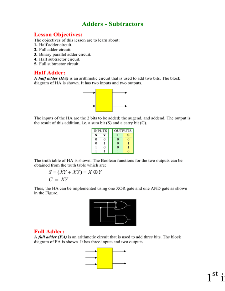
Adders - Subtractors Lesson Objectives: The objectives of this lesson are to learn about: 1. Half adder circuit. 2. Full adder circuit. 3. Binary parallel adder circuit. 4. Half subtractor circuit. 5. Full subtractor circuit. Half Adder: A half adder (HA) is an arithmetic circuit that is used to add two bits. The block diagram of HA is shown. It has two inputs and two outputs. The inputs of the HA are the 2 bits to be added; the augend, and addend. The output is the result of this addition, i.e. a sum bit (S) and a carry bit (C). INPUTS X Y 0 0 0 1 1 0 1 1 OUTPUTS C S 0 0 0 1 0 1 1 0 The truth table of HA is shown. The Boolean functions for the two outputs can be obtained from the truth table which are: S = ( XY + X Y ) = X ⊕ Y C = XY Thus, the HA can be implemented using one XOR gate and one AND gate as shown in the Figure. Full Adder: A full adder (FA) is an arithmetic circuit that is used to add three bits. The block diagram of FA is shown. It has three inputs and two outputs. The inputs of the FA are the 3 bits to be added; the augend, addend, and carry from previous lower significant position. The output is the result of this addition, i.e. a sum bit (S) and a carry bit (C). INPUTS X Y Z 0 0 0 0 0 1 0 1 0 0 1 1 1 0 0 1 0 1 1 1 0 1 1 1 OUTPUTS C S 0 0 0 1 0 1 1 0 0 1 1 0 1 0 1 1 The truth table of FA is shown. The simplified Boolean functions for the two outputs can be obtained from the truth table, which are: S = X Y Z + XY Z + X Y Z + XYZ = X ⊕Y ⊕ Z C = XY + XZ + YZ The Boolean functions for the two outputs can be manipulated to simplify the circuit, as shown below: (see animation in authorware version) S = X Y Z + XY Z + X Y Z + XYZ = X ⊕Y ⊕ Z = ( X ⊕Y ) ⊕ Z C = XY + X Y Z + X YZ = XY + Z ( X Y + X Y ) = XY + Z ( X ⊕ Y ) Thus the full adder can be implemented using two half adders and an OR gate as shown in the Figure. Binary Parallel Adder: An n-bit adder is a circuit which adds two n-bits numbers, say, A and B. In addition, an n-bit adder will have another single-bit input which is added to the two numbers called the carry-in (Cin). The output of the n-bit adder is an n-bit sum (S) and a carry-out (Cout) bit. The block diagram of the n-bit adder is shown. If all input bits of the two numbers (A & B) are applied simultaneously in parallel, the adder is termed a Parallel Adder. Consider the problem of designing a 4-bit binary parallel adder. The total number of inputs is 9, since the two numbers have 4-bits each in addition to the Cin bit. Using conventional techniques for design would require a truth table of 29=512 rows. This causes the conventional design procedure to be unacceptable in this case. Alternatively, the 4-bit binary parallel adder can be designed using 4 full adders connected in-cascade as shown in the figure. That is the carry-out bit of one full adder stage is used as carry-in input to the next stage. In general, an n-bit binary parallel adder can be built out of n full adders connected in cascade. Since a carry of 1 may appear near the least significant bit of the adder and yet propagate through many full adders to the most significant bit, just as a wave ripples outward from a pebble dropped in a pond. That is why this parallel adder is also called as ripple carry adder. The disadvantage of the ripple-carry adder is that it can get very slow when one needs to add many bits. The propagation delay of this adder is fairly long since under worst case conditions, the carry has to propagate through all the stages as shown in the figure by red colored path. This propagation delay is a limiting factor on the adder speed. The signal from the input carry to the output carry propagates through an AND gate and OR gate, which constitute two gate levels. If there are four full adders, the output carry would have 2 x 4 = 8 levels from C0 to C4. The total propagation time in this 4-bit adder would be the propagation time in one half adder (which is the first half adder) plus eight gate levels. (see animation in authorware version) Assuming that all the different types of gates have same propagation delay, say T, the propagation delay of adder can be generalized as (2n + 1) T, where n is the number of stages. In this example, n = 4, so the delay is (2 x 4 + 1) T = 9T Since all other arithematic operations are implemented by successive additions, the time consumed during addition process is very critical. For fast applications, a better design is required. The carry-look-ahead adder solves this problem by calculating the carry signals in advance, based on the input signals. It is expalined in the next lesson. Appendix: Half Subtractor: A half subtractor is an arithmetic circuit that subtracts two bits and produces their difference. The block diagram of half subtractor is shown. The circuit has two inputs minuend (X) and subtrahend (Y) and two output bits, one is the difference bit (D) and the other is the borrow bit (B). It performs the operation X – Y. It should be noted that the weight of the output borrow bit is -2, while the weight of the output difference bit is +1. INPUTS X Y 0 0 0 1 1 0 1 1 OUTPUTS B D 0 0 1 1 0 1 0 0 The truth table of the half subtractor is shown. The Boolean functions for the two outputs can be obtained directly from the truth table as: D = ( XY + X Y ) = X ⊕ Y B = XY Full Subtractor: A full subtractor is a combinational circuit that performs a subtraction between two bits, taking into account that a 1 may have been borrowed by a lower significant bit. The block diagram of full subtractor is shown. The circuit has three inputs and two outputs. Input variables are minuend (X), subtrahend (Y), and previous borrow (Z); output variables are difference (D) and output borrow (B). It performs the operation X – Y – Z. It should be noted that the weight of the output borrow bit is -2, while the weight of the output difference bit is +1. The truth table of the full subtractor is shown. INPUTS X Y Z 0 0 0 0 0 1 0 1 0 0 1 1 1 0 0 1 0 1 1 1 0 1 1 1 OUTPUTS B D 0 0 1 1 1 1 1 0 0 1 0 0 0 0 1 1 The simplified Boolean functions for the two outputs are: D = X Y Z + XY Z + X Y Z + XYZ = X ⊕Y ⊕ Z B = X Y + X Z + YZ
