Lecture Slides
advertisement

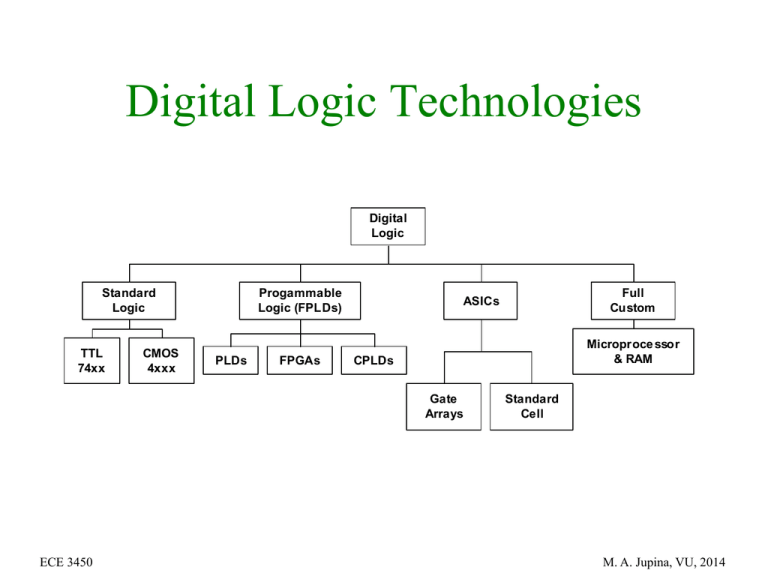
Digital Logic Technologies Digital Logic Standard Logic TTL 74xx CMOS 4xxx Progammable Logic (FPLDs) PLDs FPGAs Microproce ssor & RAM CPLDs Gate Arrays ECE 3450 Full Custom ASICs Standard Cell M. A. Jupina, VU, 2014 Some Key Lecture Objectives A discussion of how digital logic circuits can be implemented through various technologies (Discrete vs PLD vs ASIC vs Full Custom). Understand how FPLD technology is implemented by briefly looking at CPLD and FPGA architectures. Understand the advantages of FPLD technology. References: 1. Fundamentals of Digital Logic, Sections 2.9, 2.10, 3.5 – 3.7, and Appendices A-E. 2. Document files at the course web site ECE 3450 M. A. Jupina, VU, 2014 A 7400-Series Chip VDD Gnd Dual-inline package ECE 3450 Structure of 7404 chip M. A. Jupina, VU, 2014 Discrete Implementation Example VD D 7404 f = x1x 2 + x 2 x 3 7408 x1 x2 x3 ECE 3450 7432 f M. A. Jupina, VU, 2014 General Structure of a PLA x1 x2 xn Input buffers and inverters x1 x1 xn xn P1 OR plane AND plane Pk f1 ECE 3450 fm M. A. Jupina, VU, 2014 x1 x2 x3 An Example of a PLA OR plane P1 P2 P3 P4 AND plane f1 x1 x2 x1 x3 x1 x2 x3 f 2 x1 x2 x1 x2 x3 x1 x3 ECE 3450 f1 f2 M. A. Jupina, VU, 2014 An Example of a PAL x1 x2 x3 f1 x1 x2 x3 x1 x2 x3 f 2 x1 x2 x1 x2 x3 P1 f1 P2 P3 f2 P4 AND plane ECE 3450 M. A. Jupina, VU, 2014 PAL-like block PAL-like block I/O block I/O block Structure of a CPLD ECE 3450 PAL-like block PAL-like block I/O block I/O block Interconnection wires M. A. Jupina, VU, 2014 A Section of a CPLD PAL-like block (details not shown) PAL-like block D Q D Q D Q ECE 3450 M. A. Jupina, VU, 2014 Structure of a FPGA ECE 3450 M. A. Jupina, VU, 2014 Logic Block Example A two-input lookup table x1 Complete Logic Block 0/1 0/1 f 0/1 0/1 x2 (a) Circuit for a two-input LUT x1 x2 f1 0 0 1 1 1 0 0 1 0 1 0 1 (b) f 1 = x 1 x 2 + x 1 x 2 Select Out Flip-flop In 1 In 2 D LUT Q In 3 x1 Clock 1 0 f1 0 1 x2 (c) Storage cell contents in the LUT ECE 3450 M. A. Jupina, VU, 2014 A Sea-of-Gates Gate Array ECE 3450 M. A. Jupina, VU, 2014 An Example of a Logic Function in a Gate Array f1 x1 x2 x3 f1 = x 2 x 3 + x1x 3 ECE 3450 M. A. Jupina, VU, 2014 A Simplified Floor Plan of a Standard Cells Based Design ECE 3450 M. A. Jupina, VU, 2014 Standard Cell Structure All cells have same pitch (height), may have different widths. VDD, VSS (ground) connections are designed to run through cells. A feedthrough area may allow wires to be routed over the cell. VDD n tub pullups Intra-cell wiring pulldowns p tub or substrate VSS ECE 3450 M. A. Jupina, VU, 2014 Example: Full Adder Schematic Two Outputs: Sum and Carry n1 x1 n2 n4 x2 sum n3 carry ECE 3450 M. A. Jupina, VU, 2014 A Candidate Layout of a Full Adder Density = 5 a b co x1 x2 n1 n2 n3 n4 s c ECE 3450 M. A. Jupina, VU, 2014 Layout of Full Adder Cell XOR (2) ECE 3450 XOR (2) NAND NAND NAND NAND (2) (2) (2) (3) M. A. Jupina, VU, 2014 Intel Pentium (IV) Microprocessor 2001 42 million transistors 2 GHz clock ECE 3450 M. A. Jupina, VU, 2014 Emerging Chip Architecture Silicon Chip FPLD Circuits IP CORE ECE 3450 M. A. Jupina, VU, 2014 Example of a System-on-a-Chip (SOC) Architecture System-on-a-Programmable Chip (SOPC) NOW EMERGING! ECE 3450 M. A. Jupina, VU, 2014 Digital Logic Technology Tradeoff Ful Custom V LS I Design S peed, Densi ty, Complexi ty, Market V olume needed for P roduct A S ICs CP LDs FP GA s P LDs E ngn i eering Cost, Tm i e to Deveo lpP roduct ECE 3450 M. A. Jupina, VU, 2014 Comparison of Digital Technologies ECE 3450 M. A. Jupina, VU, 2014 Latest FPLD ECE 3450 M. A. Jupina, VU, 2014 FPLD Advantages 1. Re-configurable: The IC can be configured or “wired” to perform a particular task at a given instance in time and then reconfigured or “rewired” to perform another task a moment later. For example, the IC could be used as a low pass FIR digital filter one moment then reconfigured as a band pass FIR filter the next moment. ROM ROM FPLD ROM ROM 2. Rapid Prototyping 3. FPGA to ASIC Design (Example: Altera Stratix III to HardCopy III) http://www.altera.com/literature/hb/hardcopy-iii/hiii51001.pdf ECE 3450 M. A. Jupina, VU, 2014 Issues in FPLD Technologies • Complexity of Logic Element – How many inputs/outputs for the logic element? – Does the basic logic element contain a FF? What type? • Interconnect – How fast is it? Does it offer ‘high speed’ paths that cross the chip? How many of these? – Can I have on-chip tri-state busses? – How routable is the design? If 95% of the logic elements are used, can I route the design? More routing means more “route-ability,” but less room for logic elements ECE 3450 M. A. Jupina, VU, 2014 Issues in FPLD Technologies Continued • Macro elements – Are there SRAM blocks? Is the SRAM dual ported? – Is there fast adder support (i.e. fast carry chains?) – Is there fast logic support (i.e. cascade chains) – What other types of macro blocks are available (fast decoders? register files? ) • Clock support – How many global clocks can I have? – Are there any on-chip Phase Locked Loops (PLLs) or Delay Locked Loops (DLLs) for clock synchronization, clock multiplication? ECE 3450 M. A. Jupina, VU, 2014 Issues in FPLD Technologies Continued • What type of I/O support exists? – TTL, CMOS are a given – Support for mixed 5V, 3.3V I/Os? • 3.3 v internal, but 5V tolerant inputs? – Support for new low voltage signaling standards? • GTL (Gunning Transceiver Logic) - used on Pentium II • HSTL - High Speed Transceiver Logic • SSTL - Stub Series-Terminate Logic • USB - Universal Serial Bus (differential signaling) (bottom view) • AGP - Advanced Graphics Port – Maximum number of I/O? Package types? Ball Grid Array (BGA) for high density I/O ECE 3450 M. A. Jupina, VU, 2014 Examples of FPLDs and Advanced High Pin Count Package Types PLCC ECE 3450 PQFP Ceramic PGA M. A. Jupina, VU, 2014 Altera FPLD Family Summaries • Altera Max7000/Max7000A – EEPROM based, very fast (tp = 7.5 ns) – Basically a PLD architecture with programmable interconnect. – Max 7000A family is 3.3 V • Altera Flex10K/10KE – LEs (Logic elements) have 4-input LUTS (look-up tables) and 1 FF – Fast Carry Chain between LE’s and Cascade chain for logic operations – Large blocks of SRAM available as well ECE 3450 M. A. Jupina, VU, 2014 MAX 7000 Macrocell (16 inputs) (36 signals from PIA) ECE 3450 Output can be fed back to input for state machine implementation M. A. Jupina, VU, 2014 MAX 7000 LAB and PIA ECE 3450 M. A. Jupina, VU, 2014 MAX 7000 CPLD Architecture ECE 3450 M. A. Jupina, VU, 2014 FLEX 10K LE ECE 3450 M. A. Jupina, VU, 2014 FLEX 10K LAB and Interconnects ECE 3450 M. A. Jupina, VU, 2014 8-Bit Parallel Adder Example ECE 3450 M. A. Jupina, VU, 2014 Product Term of Eight Variables Example ECE 3450 M. A. Jupina, VU, 2014 FLEX 10K FPGA Architecture ECE 3450 M. A. Jupina, VU, 2014


