Microfluidic Device as a Novel Platform for the Immunofluorescent
advertisement
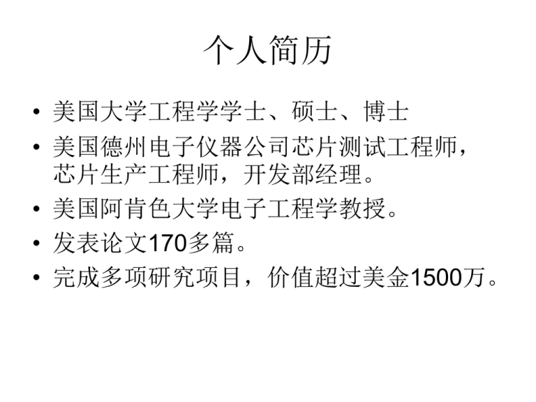
个人简历 • 美国大学工程学学士、硕士、博士 • 美国德州电子仪器公司芯片测试工程师, 芯片生产工程师,开发部经理。 • 美国阿肯色大学电子工程学教授。 • 发表论文170多篇。 • 完成多项研究项目,价值超过美金1500万。 个人简历 • 博士生导师,指导过65位博士和硕士生。 • 获得伦敦城市行业教育学会的“CGIA”文 凭。 • 写了关于开关电源技术方面的书一本,书 名为“Power Switching Converters” • 美国电解化学协会委员。 • 微电子封装研究所主任。 University of Arkansas Micro-Electro-Mechanical Devices Simon S. Ang Professor of Electrical Engineering University of Arkansas USA What is Micro-Electromechanical Device or MEMs? • Imagine machines so small they are imperceptible to the human eye. • Imagine working machines with gears no bigger than a grain of pollen. What is MEMS? • Micro-Electro-Mechanical Systems (MEMS) is the integration of mechanical elements, sensors, actuators, and electronics on a common substrate using micro-fabrication technology. MEMS Applications • Air Bag Sensor - crash-bag deployment in automobile (accelerometer) • Ink Jet Printer • Bio-MEMS – Polymerase Chain Reactor (PCR) for DNA amplification and identification MEMS Accelerometer Automotive -- Testing, Suspension, Air Bags Agricultural -- Harvesting shock & vibration, Production line monitoring Manufacturing -- Testing, Production line monitoring, Shipping monitoring Transportation -- Rail-car sensing, Shipping monitoring, Testing Down Hole Drilling -- Tilt/Attitude sensing, Machinery health NASA -- Vibration Monitoring, Testing (From Silicon Design Inc.,) A Portable PCR Device Biological Detection Technology for Counter – Terrorism (Lawrence Livermore Laboratory) Sandia’s Micro-Mirror Spider Mite on a Sandia’s MicroMirror Spider Mite Approaching a Sandia’s Micro-Gear Assembly Micro Spacecrafts Microthruster Microthruster Microcombustion testing Microthruster Thrust (N) 0.45 0.40 Wt=280 micron 0.35 Wt=260 micron 0.30 Wt=200 micron 0.25 0.20 0.15 0.10 0.05 0.00 0.00 0.05 0.10 0.15 0.20 0.25 0.30 0.35 0.40 0.45 0.50 0.55 0.60 0.65 0.70 0.75 0.80 Tim e (m s) Microthruster firing sequence Basic Surface Micromachining Process Sequence I. Deposit Sacrificial Layer IV. Pattern Mechanical Layer II. Pattern Sacrificial Layer V. Release Mechanical Layer +V III. Deposit Mechanical Layer VI. Test Device Microelectronic Fabrication Photomask Fabricated Devices Processing Equipment Processing Equipment Processing Equipment Processing Equipment Processing Equipment Processing Equipment Processing Equipment Aluminum Wire Bonder Gold Wire Bonder Wire Bond Pull Tester Measurement Equipment Microelectronic Cleanroom Operation Microelectronic Cleanroom Operation Microelectronic Cleanroom Operation Microelectronic Cleanroom Operation Microelectronic Cleanroom Operation Microelectronic Cleanroom Operation Wire Bonding Microfluidic Devices • Microfluidic devices are MEMS devices with micro-scale (10-6m) or nano-scale (10-9m) flow channels • They come with valves, electrodes, heaters, and other features • These microfluidic devices can be used as tiny chemical processing or reaction system, consuming only tiny amount of chemical – micro-TAS (micro total analysis system) Post-type Filter Comb-Type Filter Weir-type Filter Glass cover 50µm Silicon plate Inlet Outlet Weir-type Filter 50µm In Chip Immunofluorescent Cell Detection Glass cover Labeling Detection Fluorescent Microscope Silicon Plate Cell Fluorescent labeled antibody Labeled cell Beads in the Microchannels Deep channel (before filter chamber) Shallow channel (After filter chamber) Confocal Images of Microchannel Shallow channel Deep Channel Fluent Simulations of Microfilter Chip 1μm weir gap 3μm weir gap Flow rate=2 mm/s Flow rate=2mm/s 6μm weir gap Flow rate=2mm/s 9μm weir gap Flow rate=2mm/s Fluent Simulations of Microfilter Chip 1μm weir gap Depth=10μm Depth=30μm 50µm Depth=50μm Flow rate=1mm/s Flow rate=0.5mm/s Labeling efficiency along the weir 50 Depth of Weir 40 30 20 10 0 0 20 40 60 Normalized S/N ratio 80 100 120 Trapping Efficiency Comparison with the conventional detection on slides • On slides • Within filter chip – 9 steps – 3 steps – Takes more than 1 – Takes less than h 0.5h – Consumes 20µl – Consumes 2 µl cells solution and cells solution and 25 µl labeling labeling reagent reagent Pillar-Type Microfludic Filter Chip Future work • Next generation chip: – Comb-type chip – Multiplex • Application in DNA array • Application in ELISA • Incorporate QD Other Related Work • • • • • Quantum dot labeling Bacteria sensors Brain probes Recording integrated circuitries Microelectronics Packaging Quantum Dots Detection System Quantum Dots Labeling of C. parvum (red) and G. Lamblia (Green) “Quantum Dots as a Novel Immunofluorescent Detection System for Cryptosporidium parvum and Giardia lamblia,” L. Zhu, S. Ang, & WenTso Liu, in Applied and Environmental Microbiology. Interdigitated Electrode Sensor What is a Bio-Sensor? • Biologically sensitive Material Direct – Antibodies – Enzymes – DNA Probes • Transducing Element/System – Electrochemical – Optical – mass • Interfacing Indirect – Fluorescent – Chemiluminescent – Enzymatic substrate E-coli Sensing Principle Fe[(CN)6]3-/4- E. coli O157:H7 Charge transfer is blocked cells Streptavidin Self Assembled Monolayer Au Electrode Scanning Electron Micrograph of E-Coli on Bio-Sensor E-coli cells on the surface of bio-sensor before washing away non-specific binding - 65 x 100 μm window size 1000 X Magnification Surface of Electrode (AFM) Brain Sensors • Multi-site potential and chronoamperometry brain probes Neural Signal Recording Electrodes Potential Electrode Nano Interdigitated Array Electrochemical Recording Electrode Brain Sensors • A brain probe mounted and wire bonded on a circuit board carrier Brain Sensors • SEM Photo of a multi-site potential and chronoamperometry brain probe Brain Sensors • SEM Photo of a multi-site potential and chronoamperometry brain probe Silicon Microprobe Process Flow Silicon Microprobe Process Flow Brain Probe Recording in Rat’s Brain Extracellular Field Potentials in Olfactory Bulb of A Male Rat Stainless steel microwires - 100µm diameter, enamel-insulated 16-site brain microprobe A) Match in evoked potential amplitude and waveform across the four recording sites when occupying the same position in the olfactory bulb B) Sharp reversal of polarity as each recording site across the mitral cell later, indicating that crosstalk between channels is minimal. Recording Integrated Circuit Microelectronic Packaging Test & Burn-In (Wafer Level Test Active Probe Card) Microelectronic Packaging Interposer Power & USB TSP PCB Wafer Wafer Chuck uBGA Silicon or LTCC or PCB-like Compliant Thin Film Redistribution Capture/Alignment Structure Microelectronic Packaging Microelectronic Packaging Microelectronic Packaging Thank You Questions ?
