TEM - transmission electron microscopy
advertisement
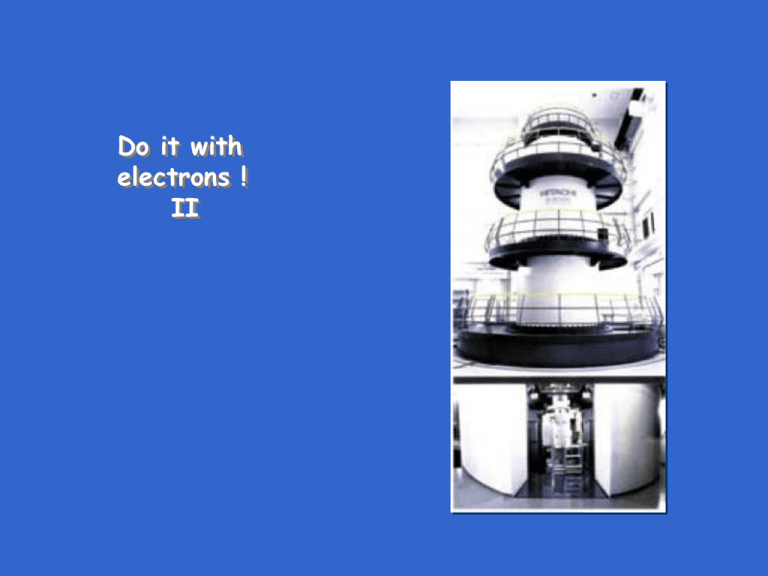
Do it with electrons ! II TEM - transmission electron microscopy Typical accel. volt. = 100-400 kV (some instruments - 1-3 MV) Spread broad probe across specimen - form image from transmitted electrons Diffraction data can be obtained from image area Many image types possible (BF, DF, HR, ...) - use aperture to select signal sources Main limitation on resolution aberrations in main imaging lens Basis for magnification - strength of post- specimen lenses TEM - transmission electron microscopy Instrument components Electron gun (described previously) Condenser system (lenses & apertures for controlling illumination on specimen) Specimen chamber assembly Objective lens system (imageforming lens - limits resolution; aperture - controls imaging conditions) Projector lens system (magnifies image or diffraction pattern onto final screen) TEM - transmission electron microscopy Instrument components Electron gun (described previously) Condenser system (lenses & apertures for controlling illumination on specimen) Specimen chamber assembly Objective lens system (imageforming lens - limits resolution; aperture - controls imaging conditions) Projector lens system (magnifies image or diffraction pattern onto final screen) TEM - transmission electron microscopy SIGNALS IN ELECTRON MICROSCOPY x-rays composition backscattered e's microstructure secondary e's microstructure inelastically scattered e's composition elastically scattered e's crystallographic structure transmitted e's microstructure TEM - transmission electron microscopy Examples Matrix - '-Ni2AlTi Precipitates - twinned L12 type '-Ni3Al TEM - transmission electron microscopy Examples Precipitation in an Al-Cu alloy TEM - transmission electron microscopy Examples dislocations in superalloy SiO2 precipitate particle in Si TEM - transmission electron microscopy Examples lamellar Cr2N precipitates in stainless steel electron diffraction pattern TEM - transmission electron microscopy Specimen preparation Types replicas films slices powders, fragments foils as is, if thin enough ultramicrotomy crush and/or disperse on carbon film Foils 3 mm diam. disk very thin (<0.1 - 1 micron - depends on material, voltage) TEM - transmission electron microscopy Specimen preparation Foils 3 mm diam. disk very thin (<0.1 - 1 micron - depends on material, voltage) mechanical thinning (grind) chemical thinning (etch) ion milling (sputter) examine region around perforation TEM - transmission electron microscopy Diffraction Use Bragg's law - = 2d sin But much smaller (0.0251Å at 200kV) if d = 2.5Å, = 0.288° TEM - transmission electron microscopy Diffraction 2 ≈ sin 2 = R/L = 2d sin ≈ d (2) specimen R/L = /d Rd = L L is "camera length" L is "camera constant" image plane TEM - transmission electron microscopy Diffraction Get pattern of spots around transmitted beam from one grain (crystal) TEM - transmission electron microscopy Diffraction Symmetry of diffraction pattern reflects symmetry of crystal around beam direction Example: 6-fold in hexagonal, 3-fold in cubic [111] in cubic [001] in hexagonal Why does 3-fold diffraction pattern look hexagonal? TEM - transmission electron microscopy Diffraction Note: all diffraction patterns are centrosymmetric, even if crystal structure is not centrosymmetric (Friedel's law) Some 0-level patterns thus exhibit higher rotational symmetry than structure has P cubic reciprocal lattice layers along [111] direction l = +1 level 0-level l = -1 level TEM - transmission electron microscopy Diffraction Cr23C6 - F cubic a = 10.659 Å Ni2AlTi - P cubic a = 2.92 Å TEM - transmission electron microscopy Diffraction - Ewald construction Remember crystallite size? when size is small, x-ray reflection is broad To show this using Ewald construction, reciprocal lattice points must have a size TEM - transmission electron microscopy Diffraction - Ewald construction Many TEM specimens are thin in one direction - thus, reciprocal lattice points elongated in one direction to rods - "relrods" Also, very small, 1/ very large Only zero level in position to reflect Ewald sphere TEM - transmission electron microscopy Indexing electron diffraction patterns Measure R-values for at least 3 reflections TEM - transmission electron microscopy Indexing electron diffraction patterns TEM - transmission electron microscopy Indexing electron diffraction patterns Index other reflections by vector sums, differences Next find zone axis from cross product of any two (hkl)s (202) x (220) ——> [444] ——> [111] TEM - transmission electron microscopy Indexing electron diffraction patterns Find crystal system, lattice parameters, index pattern, find zone axis ACTF!!! Note symmetry - if cubic, what direction has this symmetry (mm2)? Reciprocal lattice unit cell for cubic lattice is a cube TEM - transmission electron microscopy Why index? Detect epitaxy Orientation relationships at grain boundaries Orientation relationships between matrix & precipitates Determine directions of rapid growth Other reasons TEM - transmission electron microscopy Polycrystalline regions polycrystalline BaTiO3 spotty Debye rings TEM - transmission electron microscopy Indexing electron diffraction patterns - polycrystalline regions Same as X-rays – smallest ring - lowest - largest d Hafnium (铪) TEM - transmission electron microscopy Indexing electron diffraction patterns - comments Helps to have some idea what phases present d-values not as precise as those from X-ray data Systematic absences for lattice centering and other translational symmetry same as for X-rays Intensity information difficult to interpret TEM - transmission electron microscopy Sources of contrast Diffraction contrast - some grains diffract more strongly than others; defects may affect diffraction Mass-thickness contrast - absorption/ scattering. Thicker areas or mat'ls w/ higher Z are dark TEM - transmission electron microscopy Bright field imaging Only main beam is used. Aperture in back focal plane blocks diffracted beams Image contrast mainly due to subtraction of intensity from the main beam by diffraction TEM - transmission electron microscopy Bright field imaging Only main beam is used. Aperture in back focal plane blocks diffracted beams Image contrast mainly due to subtraction of intensity from the main beam by diffraction TEM - transmission electron microscopy Bright field imaging Only main beam is used. Aperture in back focal plane blocks diffracted beams Image contrast mainly due to subtraction of intensity from the main beam by diffraction TEM - transmission electron microscopy Bright field imaging Only main beam is used. Aperture in back focal plane blocks diffracted beams Image contrast mainly due to subtraction of intensity from the main beam by diffraction TEM - transmission electron microscopy What else is in the image? Many artifacts surface films local contamination differential thinning others Also get changes in image because of annealing due to heating by beam TEM - transmission electron microscopy Dark field imaging Instead of main beam, use a diffracted beam Move aperture to diffracted beam or tilt incident beam TEM - transmission electron microscopy Dark field imaging Instead of main beam, use a diffracted beam Move aperture to diffracted beam or tilt incident beam strain field contrast TEM - transmission electron microscopy Dark field imaging Instead of main beam, use a diffracted beam Move aperture to diffracted beam or tilt incident beam TEM - transmission electron microscopy Lattice imaging Use many diffracted beams Slightly off-focus Need very thin specimen region Need precise specimen alignment See channels through foil Channels may be light or dark in image Usually do image simulation to determine features of structure 铝 钌 铜 合金 TEM - transmission electron microscopy Examples M23X6 (figure at top left). L21 type '-Ni2AlTi (figure at top center). L12 type twinned 'Ni3Al (figure at bottom center). L10 type twinned NiAl martensite (figure at bottom right).
