Learning Outcome - CMOS VLSI Layout Design
advertisement
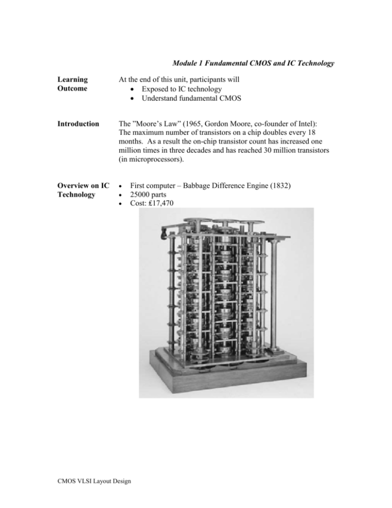
Module 1 Fundamental CMOS and IC Technology Learning Outcome At the end of this unit, participants will Exposed to IC technology Understand fundamental CMOS Introduction The ”Moore’s Law” (1965, Gordon Moore, co-founder of Intel): The maximum number of transistors on a chip doubles every 18 months. As a result the on-chip transistor count has increased one million times in three decades and has reached 30 million transistors (in microprocessors). Overview on IC Technology First computer – Babbage Difference Engine (1832) 25000 parts Cost: ₤17,470 CMOS VLSI Layout Design Module 1 Fundamental CMOS and IC Technology ENIAC ENIAC -- The first electronic computer (1946) The first electronic computer (1946) Vacuum tube based. ~18000 tubes 8,5ft height, 85ft long First transistor Designed in Bell Labs CMOS VLSI Layout Design Module 1 Fundamental CMOS and IC Technology First Integrated Circuit Bipolar logic 1960’s (TTL, ECL) Jack Kilby, Texas Instruments (1958), the monolithic integrated circuit, or microchip (patent #3,138,743), Nobel Prize in 2000 Integrated Circuit history o Invention of BJT (1948) o First silicon transistor (1954) o MOS transistor (1960) o MOS integrated circuit (1962) o DRAM cell (1968) o Intel formed (1968), AMD formed (1969) o Microprocessor invented (1971) o 32-bit microprocessors (1980) CMOS VLSI Layout Design Module 1 Fundamental CMOS and IC Technology Intel 4004 Microprocessor 1972, 1000 transistors 1 MHz operation, NMOS only Pentium processor CMOS VLSI Layout Design Module 1 Fundamental CMOS and IC Technology Moore’s Law IC Classification VLSI technology Circuit size (transistor count) Circuit technology (BJT, BiCMOS, NMOS, CMOS. Design style o standard cell o gate array o custom Size classification (historical) o <100 SSI 1963 o 100-3000 MSI 1970 o 3000-30,000 LSI 1975 o 30,000-1,000000 VLSI 1980 o >1,000000 ULSI 1990 o >1 billion GSI 2010 NMOS (N-type Metal-Oxide-Semiconductor) o Simple to design CMOS (Complementary Metal-Oxide Semiconductor) o Less power consumption o East to design BiCMOS (Bipolar CMOS) o Fast o Consume more power CMOS VLSI Layout Design Module 1 Fundamental CMOS and IC Technology IC Technology today ECL (Emitter-Coupled Logics) o Fast o Consume power o Less compact GaAs (Gallium Arsenic) o Very fast o Hard to design The ”Moore’s Law” (1965, Gordon Moore, co-founder of Intel): The maximum number of transistors on a chip doubles every 18 months. As a result the on-chip transistor count has increased one million times in three decades and has reached 30 million transistors (in microprocessors). Semiconductor memories (DRAM) reached the density of 1Gbits per chip. The increase of the transistor count is the result of reduction in the size of the smallest manufacturable feature, say, the minimum path/line width. The minimum feature size has decreased from around 10µm in the 1970s to less than 0.2µm in 2000. In order to reduce power consumption the supply voltage has been reduced from 5V to around 2V. It has been predicted that in 2009 we will have: o 200M transistors on a chip with the minimum feature size 100nm and the supply voltage 0.6–0.9V. The DRAM will have 64Gb per chip. We will be working with AMI05 and TMS035 technologies with the minimum feature size being 0.5µm and 0.35µm, respectively. Silicon (Si) is the most popular material use to build integrated circuits. Other possibilities include germanium (Ge) and gallium arsenide (GaAs). CMOS VLSI Layout Design Module 1 Fundamental CMOS and IC Technology MOS Transistor NMOS The flow of the current between the source and the drain is controlled by the electric field generated by the gate-substrate voltage. Two n+ diffusion regions (’+’ indicates the high degree of doping) form the source and drain of the transistor. The area in between forms a conducting channel. Potentially, electrons, negative carriers, will form the current in the channel. The gate, which is formed from a conductor, typically polysilicon, is insulated from the source-channel-drain structure (and from the substrate) by the layer of silicon dioxide. The voltage between the gate and the substrate induces the electric field which controls the flow of the carriers in the channel. This gives the rise to the name: field-effect transistor (FET). Transistor structure is completely symmetrical with respect to the source and drain. The role is defined by terminal voltages which establish the direction of the current (carriers) flow. CMOS VLSI Layout Design Module 1 Fundamental CMOS and IC Technology CMOS VLSI Layout Design Module 1 Fundamental CMOS and IC Technology Cut off region for an NMOS We start with case when the gate voltage, VGS is smaller than the threshold voltage, VT . The drain voltage, VDS is in this situation irrelevant and can be zero. The electric field induced by the gate voltage points down from the gate through the channel. This fields repels the majority carriers for the p-type substrate, that is, positive holes, from the channel hence forming a region depleted of carriers as shown in figure above. As a result, due to the lack of free carriers, no current flows between the source and the drain at this stage, that is, ID = 0. Conducting NMOS Source and drain are electrically connected. If VDS>0V, then electron flow from source to drain provided VGS>VT Electrons are the charge carriers for NMOS transistor. CMOS VLSI Layout Design Module 1 Fundamental CMOS and IC Technology Reference 1. Mr. A.P.Papli´nski’s lecture notes 2. http://infopad.eecs.berkeley.edu/~icdesign/. CMOS VLSI Layout Design


