EE 457 Lab 2
advertisement
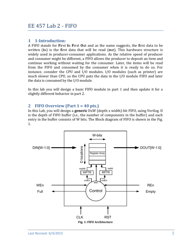
EE 457 Lab 2 - FIFO 1 1-Introduction: A FIFO stands for First In First Out and as the name suggests, the first data to be written (in) is the first data that will be read (out). This hardware structure is widely used in producer-consumer applications. As the relative speed of producer and consumer might be different, a FIFO allows the producer to deposit an item and continue working without waiting for the consumer. Later, the items will be read from the FIFO and consumed by the consumer when it is ready to do so. For instance, consider the CPU and I/O modules. I/O modules (such as printer) are much slower than CPU, so the CPU puts the data in the I/O module FIFO and later the data is consumed by the I/O module. In this lab you will design a basic FIFO module in part 1 and then update it for a slightly different behavior in part 2. 2 FIFO Overview (Part 1 = 40 pts.) In this Lab, you will design a generic DxW (depth x width)-bit FIFO, using Verilog. D is the depth of FIFO buffer (i.e., the number of components in the buffer) and each entry in the buffer consists of W bits. The Block diagram of FIFO is shown in the Fig. 1. DIN[W-1:0] D locations W-bits DOUT[W-1:0] Register Array raddr waddr WPTR cntEn RPTR wen cntEn WEn REn Control Full CLK Empty RST Fig. 1: FIFO Architecture Last Revised: 6/4/2015 1 EE 457 Lab 2 - FIFO Signal Description DIN[W-1:0], DOUT[W-1:0]: Data to be written and output read data, respectively WEn: Write Enable instructs the FIFO to write the data on DIN to the next available location in the register array if sufficient space will be available. Note the user can assert this signal even when sufficient space will not be available and your FIFO logic must NOT write/update the register array in that case (i.e. Don't assume the user will only assert this signal under appropriate conditions. REn: Read Enable indicates that the consumer is about to consume the data on DOUT and the FIFO can eventually overwrite the current data item and begin to output the next available data on the next clock edge. Full: Indicates the FIFO is currently full Empty: Indicates the FIFO is currently empty RST: Active-high reset signal Read & Write Pointers: You should access the register array using two pointers/addresses: 1- RP (Read Pointer), 2- WP (Write Pointer). RP points to the next item to be read from the memory array. WP points to the next location to be written to the memory array. Initially, both pointers start at 0. After a successful Write or Read (triggered by the user asserting WEn or REn and sufficient conditions exist to carry-out the operation), the respective pointers should increment, wrapping to 0 after the last location. Full & Empty Conditions: One complicating issue is to decipher when your FIFO is empty or full. Both conditions occur when WP = RP. For example, WP=RP=0 initially when the FIFO is empty. But if you wrote values to the FIFO, completely filling it, then WP would wrap back to 0 while RP would not have changed from 0. Thus WP=RP is an insufficient condition to decipher when the FIFO is empty or full. While several strategies exist to distinguish whether the FIFO is full or empty when RP=WP (some of which require only minimal additional logic), we suggest that you simply keep track of the number of items in your FIFO as a separate counter value and assert the Full and Empty signals appropriately using this counter value. Sufficient Write and Read Conditions: When the FIFO is full, producer should no longer be allowed to write into the FIFO even if WEn is asserted. Similarly, when the FIFO is empty, an asserted REn signal should be disregarded. Reset: When reset, initialize the necessary control logic, but we do not generally initialize the register array contents since they must be written with good data before a user can legally read any data. Verilog Considerations: We want our FIFO design to work for any number of locations (DEPTH) and bit-width (WIDTH). To do this we can declare certain 2 Last Revised: 6/4/2015 EE 457 Lab 2 - FIFO "generic parameters" (not actual physical inputs/outputs but "meta-inputs" that determine what FIFO logic is generated). In Verilog these are known as "parameters" while in VHDL they are known as "generics". Parameters can be specified when the module is instantiated and are used to create a different version of the code. In our FIFO we make the WIDTH and DEPTH parameters, in that order. Thus we can instantiate an 8-bit, 4-deep FIFO as: ee457_fifo #(8, 4) fifo4x8(clk, rst, din, wen, full, dout, ren, empty); A 16-bit, 6-deep FIFO can be instantiated as: ee457_fifo #(16, 6) fifo6x16(clk, rst, din, wen, full, dout, ren, empty); Note: Local Parameters (localparams) cannot be set when the module is instantiated and are effectively symbolic constants (like a #define in C/C++). 3 Verification of your Design We have provided a testbench for you that runs one sample sequence of operations (some legal, some illegal). You are welcome to use it as is but are STRONGLY ENCOURAGED to add/modify it to test certain aspects/corner cases of your design if our testbench does not exercise your design appropriately. You should be able to visually examine the waveform and determine if it matches the desired behavior. If not, you need to find the bug in your description and fix it. 4 Updated Design (Part 2 = 40 pts.) Once you get your initial (part 1) FIFO design working, consider a modification. Currently, if the FIFO is FULL a write can only occur AFTER a read because space needs to be freed. However, if the FIFO is FULL but a read is taking place (REN=1) then a new location will be available at the start of the next clock. Thus, we might consider allowing a write to actually occur if WEN=1 at the end of this current clock (even though the FIFO is currently FULL it won't be at the next clock edge and thus we could write). This process can continue for any number of successive clocks, meaning if the FIFO is FULL we can continue to write clock after clock as long as we also continue to read clock after clock. Copy your original file to ee457_fifo_p2.v and modify your design. Leave the module name the same so that when you compile your testbench it will just use whatever FIFO design you compiled last. 5 Procedure 1. Download the skeleton FIFO file (ee457_fifo.v) and completed testbench fie (ee457_fifo_tb.v). 2. With your understanding of the Part 1 FIFO design, complete the Verilog description. Last Revised: 6/4/2015 3 EE 457 Lab 2 - FIFO 3. Compile and simulate using the provided testbench which will instantiate an 8-bit, 4-deep FIFO, comparing the waveform to that of what you know in your mind to be the correct behavior. Remember in the objects pane of the simulation window you can click on the fifo instance and drag internal FIFO signals to the waveform window and then run the simulation (220 ns should be enough) so that you can see internal signals like 'rptr', 'wptr', etc. Feel free to modify the testbench to test any cases of input/state that are not reached from the current code. 4. Go back and change the test bench to instantiate a deeper FIFO (say, 6deep) and ensure your design still works by simulating again. 5. Copy your ee457_fifo.v to ee457_fifo_p2.v. 6. Update ee457_fifo_p2.v to implement the updated FIFO design that allows for writing when the FIFO is full but REN is enabled. 7. Recompile and simulate using your new file and ensure the design now works under these new circumstances. Feel free to modify the testbench to test any cases of input/state that are not reached from the current code. 6 Review Questions (20 pts.) 1. (5 pts.) Some FIFO users prefer to replace the "Full" and "Empty" signals with "Space Available" and "Data Available" signals to indicate there is room to write a new value or there is a value available to read, respectively. Given that you can NOT change your original design, what additional logic could you add at the periphery of your FIFO to adapt it to this new set of signals? 2. (10 pts.) In your part 1 FIFO design, were your FULL and EMPTY signals Mealy or Moore style outputs? Support your answer with 2-3 sentences of explanation: 3. (5 pts.) In the original part 1 FIFO design, if the producer asserts WEN when the FIFO is full, it would know that its request would be denied and thus would have to wait to write the value. Essentially, the producer could just look at FULL to know if its write would be accepted. In your part 2 FIFO design, can the producer continue just look at FULL to know if its write request was processed? If so, please explain briefly. If not, suggest what the producer would use (examine) to know if its write request was processed. 4 Last Revised: 6/4/2015 EE 457 Lab 2 - FIFO 7 Submission Submit a .ZIP file with your two design files and the provided testbench (or testbenches if you created others). Also submit a PDF or text file with your answers and explanations to the Review Questions. Last Revised: 6/4/2015 5
