Coatings on Plastics — Technology Designed for a Wide Range of
advertisement

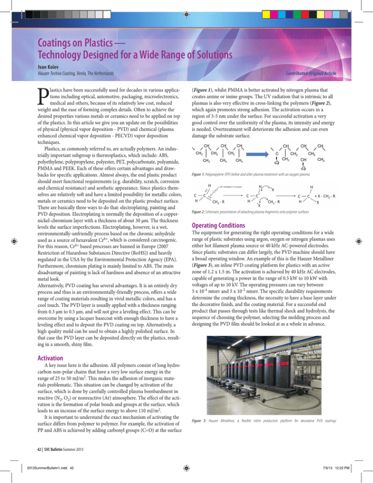
Coatings on Plastics — Technology Designed for a Wide Range of Solutions Ivan Kolev Contributed Original Article Hauzer Techno Coating, Venlo, The Netherlands P lastics have been successfully used for decades in various applications including optical, automotive, packaging, microelectronics, medical and others, because of its relatively low cost, reduced weight and the ease of forming complex details. Often to achieve the desired properties various metals or ceramics need to be applied on top of the plastics. In this article we give you an update on the possibilities of physical (physical vapor deposition - PVD) and chemical (plasma enhanced chemical vapor deposition - PECVD) vapor deposition techniques. Plastics, as commonly referred to, are actually polymers. An industrially important subgroup is thermoplastics, which include: ABS, polyethylene, polypropylene, polyester, PET, polycarbonate, polyamide, PMMA and PEEK. Each of these offers certain advantages and drawbacks for specific applications. Almost always, the end plastic product should meet functional requirements (e.g. durability, scratch, corrosion and chemical resistance) and aesthetic appearance. Since plastics themselves are relatively soft and have a limited possibility for metallic colors, metals or ceramics need to be deposited on the plastic product surface. There are basically three ways to do that: electroplating, painting and PVD deposition. Electroplating is normally the deposition of a coppernickel-chromium layer with a thickness of about 30 µm. The thickness levels the surface imperfections. Electroplating, however, is a wet, environmentally-unfriendly process based on the chromic anhydride used as a source of hexavalent Cr6+, which is considered carcinogenic. For this reason, Cr6+ based processes are banned in Europe (2007 Restriction of Hazardous Substances Directive (RoHS)) and heavily regulated in the USA by the Environmental Protection Agency (EPA). Furthermore, chromium plating is mainly limited to ABS. The main disadvantage of painting is lack of hardness and absence of an attractive metal look. Alternatively, PVD coating has several advantages. It is an entirely dry process and thus is an environmentally-friendly process, offers a wide range of coating materials resulting in vivid metallic colors, and has a cool touch. The PVD layer is usually applied with a thickness ranging from 0.3 µm to 0.5 µm, and will not give a leveling effect. This can be overcome by using a lacquer basecoat with enough thickness to have a leveling effect and to deposit the PVD coating on top. Alternatively, a high quality mold can be used to obtain a highly polished surface. In that case the PVD layer can be deposited directly on the plastics, resulting in a smooth, shiny film. (Figure 1), whilst PMMA is better activated by nitrogen plasma that creates amine or imine groups. The UV radiation that is intrinsic to all plasmas is also very effective in cross-linking the polymers (Figure 2), which again promotes strong adhesion. The activation occurs in a region of 3-5 nm under the surface. For successful activation a very good control over the uniformity of the plasma, its intensity and energy is needed. Overtreatment will deteriorate the adhesion and can even damage the substrate surface. Figure 1: Polypropylene (PP) before and after plasma treatment with an oxygen plasma Figure 2: Schematic presentation of attaching plasma fragments onto polymer surfaces Operating Conditions The equipment for generating the right operating conditions for a wide range of plastic substrates using argon, oxygen or nitrogen plasmas uses either hot filament plasma source or 40 kHz AC-powered electrodes. Since plastic substrates can differ largely, the PVD machine should have a broad operating window. An example of this is the Hauzer Metalliner (Figure 3), an inline PVD coating platform for plastics with an active zone of 1.2 x 1.5 m. The activation is achieved by 40 kHz AC electrodes, capable of generating a power in the range of 0.5 kW to 10 kW with voltages of up to 10 kV. The operating pressures can vary between 5 x 10⁻⁴ mtorr and 5 x 10⁻² mtorr. The specific durability requirements determine the coating thickness, the necessity to have a base layer under the decorative finish, and the coating material. For a successful end product that passes through tests like thermal shock and hydrolysis, the sequence of choosing the polymer, selecting the molding process and designing the PVD film should be looked at as a whole in advance. Activation A key issue here is the adhesion. All polymers consist of long hydrocarbon non-polar chains that have a very low surface energy in the range of 25 to 50 mJ/m2. This makes the adhesion of inorganic materials problematic. This situation can be changed by activation of the surface, which is done by carefully controlled plasma bombardment in reactive (N2, O2) or nonreactive (Ar) atmosphere. The effect of the activation is the formation of polar bonds and groups at the surface, which leads to an increase of the surface energy to above 110 mJ/m2. It is important to understand the exact mechanism of activating the surface differs from polymer to polymer. For example, the activation of PP and ABS is achieved by adding carbonyl groups (C=O) at the surface Figure 3: Hauzer Metalliner, a flexible inline production platform for decorative PVD coatings 42 | SVC Bulletin Summer 2013 2013SummerBulletin1.indd 42 7/9/13 12:22 PM Melting Temperature One of the reasons for the wide spread of ABS is the fact that it can be electroplated. Replacing the electroplating with PVD opens the possibility for polymers that have a higher melting temperature, can be more easily produced with a polished finish, and have better performance in combination with PVD. The higher melting temperature is directly related to the productivity of the PVD coating process. For example, replacing ABS, which can sustain a maximum of 65°C with PA66, which easily sustains 250°C, can reduce the process time by factor 2.5 for a 1.5 µm thick coating. PVD in combination with PECVD also offers the possibility of applying a thin transparent topcoat that further improves the scratch resistance without deterioration of the color. This topcoat is plasma deposited from a siloxane (HMDSO) precursor. It can be an optional final step after activation and metallization and it uses the same technology as the activation in a wide operating window. The coating from the siloxane has a low surface energy leading to strong hydrophobic properties with contact angles exceeding 90 degrees (Figure 4). This improves the fingerprint resistivity of the coating. By selecting the right process parameters, the contact angle can be gradually altered. Micro Cracks Electroplating on plastics and PVD coating on plastics remain different in terms of end properties. Electroplating produces Cr layers without distinctive morphology whereas PVD deposited Cr on plastics has a characteristic network of micro cracks (Figure 5). Their origin is related to the columnar structure of the PVD films. Their density can be reduced by optimizing the process parameters, but they cannot be avoided completely. These micro cracks account for the fact that the PVD Cr is always a bit less bright than electroplated Cr. Expressed in the (L, a*, b*) system of colors, the PVD Cr has L < 80, whereas electroplated Cr can have L = 84. In terms of mechanical properties, however, the columnar structure of the PVD film handles mechanical loads better as applied during indentation tests. Decorative PVD coatings can also be applied on top of already electroplated plastics. In this way the very limited number of metallic color finishes of the electroplating can be upgraded to the full range of colors available with PVD. Conclusion There are various options to use PVD technology as a decorative coating on plastics. If electroplating is used, PVD coating can be an excellent top layer. When electroplating needs to be avoided, solutions such as a lacquer basecoat with PVD or PVD coating directly on the plastics in batch or inline production platforms may be used. About the Author Ivan Kolev Ivan Kolev graduated from Sofia University with a M.Sc. in Semiconductor Physics in 1992 and earned a Ph.D. in Plasma Physics in 2006 from the University of Antwerp, where he specialized in numerical simulations of magnetron discharges. After graduation he held a postdoc appointment studying cold wall chemical vapour deposition. In 2008 Ivan joined Hauzer Techno Coating BV as a Senior process engineer and became Process manager for Decorative coatings. For further information, contact Ivan Kolev at Hauzer Techno Coating, at ikolev@hauzer.nl Figure 4: Contact angle – water droplet on top of hydrophobic coating Figure 5: (left) electroplated Cr layer; (middle and right) influencing the process parameters to minimize the cracks Summer 2013 SVC Bulletin | 43 2013SummerBulletin1.indd 43 7/9/13 12:22 PM


