Course Outline - UMT Admin Panel
advertisement
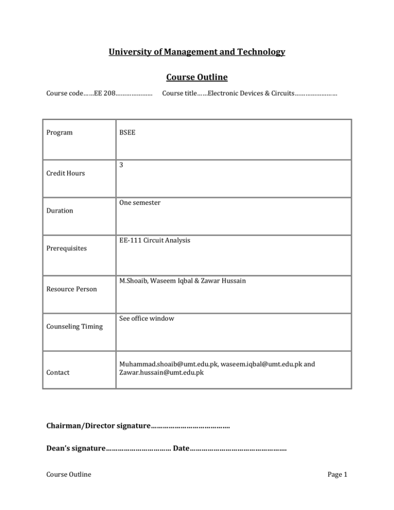
University of Management and Technology Course Outline Course code……EE 208………………… Program Credit Hours Duration Prerequisites Resource Person Counseling Timing Contact Course title……Electronic Devices & Circuits…………………… BSEE 3 One semester EE-111 Circuit Analysis M.Shoaib, Waseem Iqbal & Zawar Hussain See office window Muhammad.shoaib@umt.edu.pk, waseem.iqbal@umt.edu.pk and Zawar.hussain@umt.edu.pk Chairman/Director signature…………………………………. Dean’s signature…………………………… Date…………………………………………. Course Outline Page 1 Learning Objective: Upon Completion of the course, the students will be able to:1. 2. 3. 4. 5. 6. 7. 8. 9. Understand distinguishing characteristics of BJTs, MOSFETS ans CMOS Understand basic electronic devices e.g., diode, transistor construction and characteristics DC biasing of transistors DC biasing of FETs solve simple circuits using diodes, transistors , MOSFETS & CMOS load line analysis of diode, transistors and MOSFETS solving problems related to amplification using transistors and MOSFETS. working of a transistor and MOSFET as a switch for digital circuits Able to design electronic circuits to meet given specs Learning Methodology: Lecture, interactive, participative Grade Evaluation Criteria Following is the criteria for the distribution of marks to evaluate final grade in a semester. Marks Evaluation percentage Marks in Quizzes 15 Mid Term 25 Term Project 10 Final exam 50 Total Course Outline 100 Page 2 Recommended Text Books: Recommended Books: Text book: Electronics Devices and Circuit Theory by Robert L. Boylestad/LNashelsky ,Tenth edition Reference Books: 1) Electronic Devices by Thomas L Floyd. Ninth edition 2) Microelectronics Circuits by Sedra/Smith. Fifth edition 3) Electronics Devices and Circuit Prentice Hall, by Guillermo Rico, Jeffrey , Bogart) Sixth edition Calendar of Course contents to be covered during semester Textbook (topics) Week Course Contents Introduction to electronic devices and circuits, Semiconductor TB : 1.1-1.5 materials 1 Semiconductor Diode, Ideal versus practical TB: 1.6-1.9 Resistance Levels, Diode Equivalent circuits 2 Course Outline Page 3 Transition and diffusion capacitance, reverse recovery time, TB: 1.10-1.16 diode specification sheets, diode notation, diode testing Zener Diodes, LEDs 3 Introduction, Load line analysis of diode, diode series TB: 2.1-2.7 parallel configurations, AND/OR gates and Sinusoidal 4 Inputs: Half /Full wave rectification Clamper Circuits TB: 2.8-2.9 Clipper circuits 5 AC plus DC analysis of diode circuits (superposition principle) TB: 2.10-2.11 Zener diode (as a regulator) 6 BJT, construction, Operation, Common Base Configuration, TB: 3.1-3.10 transistor amplifying action, Common Emitter 7 configurations, Common Collector Configurations, Limits of operations, transistor specification sheets, transistor testing Mid Term Examination 8 Course Outline Page 4 Introduction, operating point, fixed biased configuration, TB: 4.1-4.8 emitter biased configuration, voltage divider biased 9 configuration, collector feedback configuration, emitter follower configuration, common base configuration Miscellaneous Bias configurations, Design Operations, TB: 4.9, 4.11, 4.16 Transistor switching networks, 10 BJT AC analysis, BJT transistor Modeling, The re transistor TB: 5.1-5.6 model for common base and common emitter configurations, 11 Common Emitter fixed bias configurations, Voltage divider bias CE Emitter-Bias configurations, Emitter follower TB: 5.7-5.11, 5.16, Configuration, Collector feedback ,collector dc feedback 5.19, 5.22 configuration, Cascaded systems, Hybrid model 12 Introduction, construction and characteristics of JFETs, transfer characteristics, important relationships, depletion and enhancement type MOSFET, CMOS TB: 6.1-6.3, 6.6-6.8 and 6.11 13 Course Outline Page 5 Introduction, fixed biased configuration, self biased TB: 7.1-7.6 configuration, voltage divider biased configuration, common gate configuration, special case 14 Depletion type MOSFETs, Enhancement type MOSFETs TB: 7.7-7.8 15 Course Outline Page 6
