Work Experience - Chabot College
advertisement
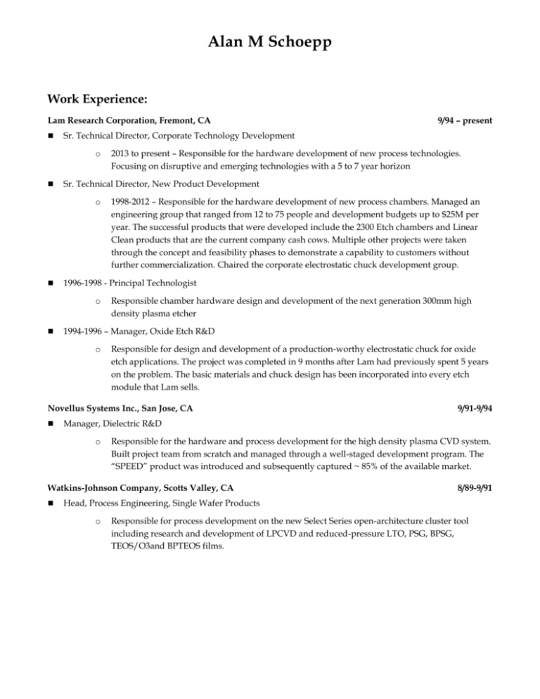
Alan M Schoepp Work Experience: Lam Research Corporation, Fremont, CA Sr. Technical Director, Corporate Technology Development o 1998-2012 – Responsible for the hardware development of new process chambers. Managed an engineering group that ranged from 12 to 75 people and development budgets up to $25M per year. The successful products that were developed include the 2300 Etch chambers and Linear Clean products that are the current company cash cows. Multiple other projects were taken through the concept and feasibility phases to demonstrate a capability to customers without further commercialization. Chaired the corporate electrostatic chuck development group. 1996-1998 - Principal Technologist o 2013 to present – Responsible for the hardware development of new process technologies. Focusing on disruptive and emerging technologies with a 5 to 7 year horizon Sr. Technical Director, New Product Development o Responsible chamber hardware design and development of the next generation 300mm high density plasma etcher 1994-1996 – Manager, Oxide Etch R&D o Responsible for design and development of a production-worthy electrostatic chuck for oxide etch applications. The project was completed in 9 months after Lam had previously spent 5 years on the problem. The basic materials and chuck design has been incorporated into every etch module that Lam sells. Novellus Systems Inc., San Jose, CA 9/91-9/94 Manager, Dielectric R&D o Responsible for the hardware and process development for the high density plasma CVD system. Built project team from scratch and managed through a well-staged development program. The “SPEED” product was introduced and subsequently captured ~ 85% of the available market. Watkins-Johnson Company, Scotts Valley, CA 9/94 – present 8/89-9/91 Head, Process Engineering, Single Wafer Products o Responsible for process development on the new Select Series open-architecture cluster tool including research and development of LPCVD and reduced-pressure LTO, PSG, BPSG, TEOS/O3and BPTEOS films. Alan M Schoepp - Page 2 Silicon Systems Inc., Santa Cruz, CA Sr. Equipment Engineer o Responsible for sustaining engineering of the epitaxial, polysilicon, and oxide CVD equipment in the thin film section of the fab. Focus Semiconductor Systems, Sunnyvale, CA 8/88-2/89 Process Technology Manager o Responsible for directing all phases of process technology including research and development, customer demonstrations, and machine qualifications for a start-up semiconductor equipment company. Watkins-Johnson Company, Scotts Valley, CA 2/89-8/89 7/84-8/88 Head, CVD Production Process and Member of the Technical Staff o 1987-88 – Designed APCVD system for deposition of tungsten-based thin films. Directed process development efforts on WSi, W, and selective W thin films. o 1986- Project manager for and chief designer for WJ-999 series of APCVD systems. This product went onto capture 85% of the available BPSG market and resulted in approximately $1B in sales over the next 10 years. o 1984-85 – Designed and managed the build of the first R&D CVD demonstration lab. Responsible for chamber design, customer demos and process development activities within the new lab. Education: Stanford University, M.S. in Mechanical Engineering 1984 Major emphases’ in high temperature gas dynamics and product design University of Missouri-Rolla, B.S. in Mechanical Engineering General Motors Scholarship recipient, emphases’ in heat transfer and thermodynamics Additional Information: 25+ granted patents in semiconductor processes and equipment design; others still pending Member of Tau Beta Pi (Engineering Honor Fraternity) Member of Pi Tau Sigma (Mechanical Engineering Honor Fraternity) 1982
