INUP
advertisement
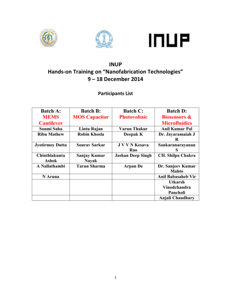
INUP Hands-on Training on “Nanofabrication Technologies” 9 – 18 December 2014 Participants List Batch A: MEMS Cantilever Batch B: MOS Capacitor Batch C: Photovoltaic Batch D: Biosensors & Microfluidics Soumi Saha Ribu Mathew Lintu Rajan Robin Khosla Varun Thakur Deepak K Jyotirmoy Dutta Sourav Sarkar Chinthlakunta Ashok A Nallathambi Sanjay Kumar Nayak Tarun Sharma J V V N Kesava Rao Jashan Deep Singh Anil Kumar Pal Dr. Jayaramaiah J R Sankaranarayanan S CH. Shilpa Chakra Arpan De N Aruna 1 Dr. Sanjeev Kumar Mahto Anil Babasaheb Vir Utkarsh Vinodchandra Pancholi Anjali Chaudhary INUP Hands-on Training on “Nanofabrication Technologies” 9th December to 18th December 2014 Program Schedule 9th December 2014 Tuesday (2nd Floor Conference Room) Time Event 8.00 AM - 9.00 AM Breakfast @CeNSE (TF-08) 9.00 AM – 10.00 AM Registration (Ground Floor Reception) 10.00 AM – 11.00 AM 11.00 AM – 1.00 PM Cleanroom protocols & Safety Training – Dr. Savitha Overview of device modules – Smitha Nair/Sangeeth K 1.00 PM – 2.30 PM Lunch and Interaction 2.30 PM - 3.30 PM About MNCF - Dr. Girish Kunte 3.30 PM - 4.15 PM Dr. Prabhakar, about execution of project proposal at CeNSE (Technical Information) Tea Break Clean Room Safety Training Quiz 4.15 PM - 4.30 PM 4.30 PM – 5.00 PM 10th December 2014 Wednesday 8.00 AM - 9.00 AM Batch C Photovoltaic: Time 9:30 AM – 1.30 PM Step 1: (9:30- 10:30) Wafer Cleaning Step 2 : (10:30 – 11:30) Wet Oxidation Step 3: (11:30-12:00) Measurement Step 4: ( 12:00 - 1:30 ) Lithography for diffusion, backside PR coating Tea and Breakfast Batch B MOS Capacitor Time 9:30 AM – 1.30 PM Training SEM Batch A MEMS: Cantilever Time 9:30 AM – 1.30 PM Step 1: (9:30- 10:30) Wafer Cleaning Batch D PDMS Microchannel Time 9:30 AM – 1.30 PM Training DC Probe Step 2: (10:30 -1:00 )EVG Lithography (for Cantilever) And Inspection 1.30 PM -2.30 PM: Lunch and Interaction Batch C Time: 2:30 PM – 5.00 PM Step 5 : (2:30 -3 :30)Oxide Etching + PR strip Batch B Time: 2.30 PM – 5.00 PM Training DC probe Introduction to other bay 5:00 PM – 5:30 PM Batch A Time: 2.30 PM – 5.00 PM Step 3: (2:00 -3:30) RIE Etching Silicon Step 4: (3:30 -5:00) PR Removal and inspection Tea Break 2 Batch D Time: 2.30 PM – 5.00 PM Training SEM 11th December 2014 Thursday 8.00 AM - 9.00 AM Batch C Time: 9:30 AM – 1.30 PM Step 6 : (9:30 – 10:30) wafer cleaning (RCA) Tea and Breakfast Batch B Time: 9:30 AM – 1.30 PM Training AFM Step 6: (10:30 - 2:30) POCL3 Diffusion Batch A Time: 9:30AM – 1.30 PM Step 5: (9:30 – 11:00)Wet OXIDE etching Batch D Time: 9:30 AM – 1.30 PM Other small Equipments Step 6: (11:00 -1:00)CPD 1.30 PM -2.30 PM: Lunch and Interaction Batch C Time 2.30PM – 5.00 PM Batch B Time: 2.30PM – 5.00 PM Batch A Time: 2.30PM – 5.00 PM Batch D Time: 2.30PM – 5.00 PM Step 7: ( 2:30 - 3:30)PSG etching Step 8: (3:30 - 4:00) four probe measurement (sheet resistance ) Step 9: (4:00 – 4:30) wafer front side PR coating Step 10: (4:30 – 5:00) back oxide etch 5:00 PM – 5:30 PM Other small Equipments Introduction to other tools (not included in the module) Training AFM Tea Break 3 12th December 2014 Friday 8.00 AM - 9.00 AM Batch C Time 9:30 AM - 1:30 PM Step 11: Front Al evaporation Step 12: (9:30 – 10:30) Lithography (contact pads) Step 13: (10:30 -11:00) wet Al etch Step 14: (11:00 – 11:30) back oxide etch Step 15: (11:30 – 1:00) back Al evaporation Unloading at 2:30 Tea and Breakfast Batch B Time: 9:30 AM- 1:30 PM Step 1: (9:30 -10:30)RCA cleaning Batch A Time 9:30 AM – 1.00 PM Characterization (Vibrometer) Step 2: (10:30 – 11:30)Dry Oxidation (SiO2) Note: samples need to be prepared earlier Batch D Time 9:30 AM – 1.00 PM Step 1: (9:30- 10:00)Wafer Cleaning (piranha) Step 2: (10:00- 11:00)Oxide layer growth Step 3: (11:00 – 12:00) Lithography Ellipsometer Step 3 : (11:30 -12:30) PR spinning + Etching of backside oxide (Load for evaporation parallel in the morning) 1.30 PM -2.30 PM: Lunch and Interaction Batch C Time 2.30PM – 5.00 PM Step 16: (3:30 -4 :30 ) annealing Batch B Time 2.30 PM – 5.00 PM Step 4: Front metallization Batch A Time 2.00PM – 5.00 PM Optical Profilometer Step 5: Lithography Step 5: (3:30 – 4:30 ) DRIE silicon etch Step 6: Metal etch 5:00 PM – 5:30 PM Batch D Time 2.30 PM – 5.00 PM Step 4: (2:30 – 3:30) Oxide etching ( dry) + Ashing Tea Break 4 15th December 2014 Monday 8.00 AM - 9.00 AM Batch C Time 9:30 AM – 1.30 PM Characterization : Tea and Breakfast Batch B Time: 9:30 AM- 1:30 PM Step 7: native oxide removal Batch A Time 9:30 AM – 1.00 PM Training DC Probe station Batch D Time 9:30AM – 1.30 PM Step 6: PDMS coating Dc probe station Step 8: back metal evaporation 1.30 PM -2.30 PM: Lunch and Interaction Batch C Time 2.30 PM – 5.00 PM Batch B Time 2.30 PM – 5.00 PM Batch A Time 2.00 PM – 5.00 PM Batch D Time 2.00 PM – 5.30 PM Characterization : Step 6: (2:30- 3:30) Annealing Training other small equipments Step 7: (2:00 -2:30) Glass piranha clean Solar simulator Introduction to other bays Step 8: (2:30-3:00)PDMS Peeling Step 9: (3:00-5:00) Bonding 5:00 PM – 5:30 PM Tea Break 16th December 2014 Tuesday 8.00 AM - 9.00 AM Batch C Time 9:30 AM – 1.00 PM Training AFM Tea and Breakfast Batch B Time 9:30AM – 1.00 PM Electrical Characterization Batch A Time 9:30 AM – 1.00 PM Training SEM Batch D Time 9:30 AM – 1.00 PM Characterization 1.30 PM -2.30 PM: Lunch and Interaction Batch C Time 2:30pm-5pm Training SEM Batch B Time 2:30pm-5pm Training AFM 5:00 PM – 5:30 PM Tea Break Batch A Time 2pm-5pm Training AFM 5 Batch D Time 2pm-5pm Characterization 17th December 2014 Wednesday (Second Floor Conference Room) 8.00 AM - 9.00 AM Tea and Breakfast 9:00 AM onwards Presentation by Participants 1:00 PM – 2:00 PM Lunch and Interaction 2:00 PM onwards Presentation by Participants & Lab Visits 18th December 2014 Thursday (Second Floor Conference Room) 8.00 AM - 9.00 AM Tea and Breakfast 9:00 AM onwards Lab Tours 1:00 PM – 2:00 PM Lunch and Interaction 2:00 PM onwards TA distribution/ Feedback/Concluding Session/ Certificate Distribution 6
