Keynote Speakers personal curriculum vitae (CV) Satoru Takahashi
advertisement
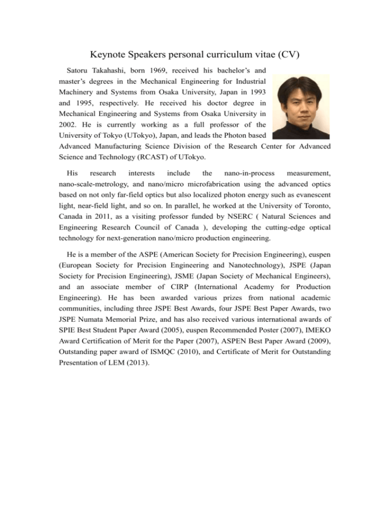
Keynote Speakers personal curriculum vitae (CV) Satoru Takahashi, born 1969, received his bachelor’s and master’s degrees in the Mechanical Engineering for Industrial Machinery and Systems from Osaka University, Japan in 1993 and 1995, respectively. He received his doctor degree in Mechanical Engineering and Systems from Osaka University in 2002. He is currently working as a full professor of the University of Tokyo (UTokyo), Japan, and leads the Photon based Advanced Manufacturing Science Division of the Research Center for Advanced Science and Technology (RCAST) of UTokyo. His research interests include the nano-in-process measurement, nano-scale-metrology, and nano/micro microfabrication using the advanced optics based on not only far-field optics but also localized photon energy such as evanescent light, near-field light, and so on. In parallel, he worked at the University of Toronto, Canada in 2011, as a visiting professor funded by NSERC ( Natural Sciences and Engineering Research Council of Canada ), developing the cutting-edge optical technology for next-generation nano/micro production engineering. He is a member of the ASPE (American Society for Precision Engineering), euspen (European Society for Precision Engineering and Nanotechnology), JSPE (Japan Society for Precision Engineering), JSME (Japan Society of Mechanical Engineers), and an associate member of CIRP (International Academy for Production Engineering). He has been awarded various prizes from national academic communities, including three JSPE Best Awards, four JSPE Best Paper Awards, two JSPE Numata Memorial Prize, and has also received various international awards of SPIE Best Student Paper Award (2005), euspen Recommended Poster (2007), IMEKO Award Certification of Merit for the Paper (2007), ASPEN Best Paper Award (2009), Outstanding paper award of ISMQC (2010), and Certificate of Merit for Outstanding Presentation of LEM (2013). ISMTII 2015 Keynote Speaker Abstract Topic: Challenge of Spatial Resolution Improvement of Optical Measurement Method Based on Localized Light Energy Abstract: In the micro manufacturing field, in-process optical inspection plays one of the most important roles for manufacturing the advanced products with high reliability, because it has several practical advantages typified by nondestructiveness, high-throughput characteristics, and so on. Optical measurement method, however, essentially restrict its spatial resolution due to the diffraction limit, which means that finer structures less than half of the wavelength of optical wave from the objects to be inspected, cannot be observed. This resolution limit of the optical measurement method is a big problem especially for the next-generation manufacturing process, where the functions of submicrometer fine structures should be more important. This critical limit about spatial resolution can be physically explained by focusing on light energy localization property. Light energy can be mainly classified in the following three types of localizations: (1) Evanescent light generated under the total internal reflection. (2) Near-field light existing in the vicinity of the bulk materials. (3) Interference intensity distribution of freely propagating light such as standing wave (mainly generated with two beam interference), focusing beam (generated with multiple beam interference), and so on. Physical principles for spatial resolution improvement are different based on types of light energy localization. In order to develop the effective optical inspection beyond the diffraction limit, it is important to recognize their super resolution property of depending on their light energy localization. In this talk, I would like to present the challenge of the spatial resolution improvement of optical measurement using various types of localized light energy, which can be applied to the micro manufacturing process inspection, and discuss their possibility for the next-generation microstructure manufacturing.
