Document
advertisement
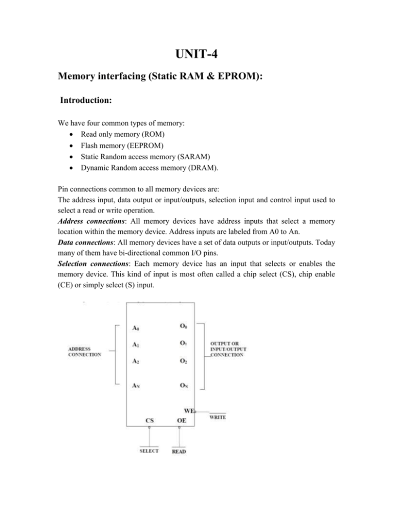
UNIT-4 Memory interfacing (Static RAM & EPROM): Introduction: We have four common types of memory: Read only memory (ROM) Flash memory (EEPROM) Static Random access memory (SARAM) Dynamic Random access memory (DRAM). Pin connections common to all memory devices are: The address input, data output or input/outputs, selection input and control input used to select a read or write operation. Address connections: All memory devices have address inputs that select a memory location within the memory device. Address inputs are labeled from A0 to An. Data connections: All memory devices have a set of data outputs or input/outputs. Today many of them have bi-directional common I/O pins. Selection connections: Each memory device has an input that selects or enables the memory device. This kind of input is most often called a chip select (CS), chip enable (CE) or simply select (S) input. MEMORY COMPONENT ILLUSTRATING THE ADDRESS, DATA AND CONTROL CONNECTIONS RAM memory generally has at least one CS or S input and ROM at least one CE If the CE, CS, S input is active the memory devices performs the read or write. If it is inactive the memory device cannot perform read or write operation. If more than one CS connection is present, all most be active to perform read or write data. Control connections: A ROM usually has only one control input, while a RAM often has one or two control inputs. The control input most often found on the ROM is the output enable (OE) or gate (G), this allows data to flow out of the output data pins of the ROM. If OE and the selected input are both active, then the output is enable, if OE is inactive, the output is disabled at its high-impedance state. The OE connection enables and disables a set of three-state buffer located within the memory device and must be active to read data. A RAM memory device has either one or two control inputs. If there is one control input it is often called R/W. This pin selects a read operation or a write operation only if the device is selected by the selection input (CS). If the RAM has two control inputs, they are usually labeled WE or W and OE or G. (WE) write enable must be active to perform a memory write operation and OE must be active to perform a memory read operation. When these two controls WE and OE are present, they must never be active at the same time. The ROM read only memory permanently stores programs and data and data was always present, even when power is disconnected. It is also called as nonvolatile memory. EPROM (erasable programmable read only memory) is also erasable if exposed to high intensity ultraviolet light for about 20 minutes or less, depending upon the type of EPROM. We have PROM (programmable read only memory). RMM (read mostly memory) is also called the flash memory. The flash memory is also called as an EEPROM (electrically erasable programmable ROM), EAROM (electrically alterable ROM), or a NOVROM (nonvolatile ROM). These memory devices are electrically erasable in the system, but require more time to erase than a normal RAM. EPROM contains the series of 27XXX contains the following part numbers: 2704(512 * 8), 2708(1K * 8), 2716(2K * 8), 2732(4K * 8), 2764(8K * 8), 27128(16K * 8) etc. Each of these parts contains address pins, eight data connections, one or more chip election inputs (CE) and an output enable pin (OE). This device contains 11 address inputs and 8 data outputs. If both the pin connection CE and OE are at logic 0, data will appear on the output connection. If both the pins are not at logic 0, the data output connections remain at their high impedance or off state. To read data from the EPROM Vpp pin must be placed at logic 1. Static RAM memory device retain data for as long as DC power is applied. Because no special action is required to retain stored data, these devices are called as static memory. They are also called volatile memory because they will not retain data without power. The main difference between a ROM and RAM is that a RAM is written under normal operation, while ROM is programmed outside the computer and is only normally read. The SRAM stores temporary data and is used when the size of read/write memory is relatively small. The control inputs of this RAM are slightly different from those presented earlier. The OE pin is labeled G, the CS pin S and the WE pin. This 4016 SRAM device has 11 address inputs and 8 data input/output connections. Static RAM Interfacing: The semiconductor RAM is broadly two types – Static RAM and Dynamic RAM. The semiconductor memories are organized as two dimensional arrays of memory locations. For example 4K * 8 or 4K byte memory contains 4096 locations, where each locations contains 8-bit data and only one of the 4096 locations can be selected at a time. Once a location is selected all the bits in it are accessible using a group of conductors called Data bus. For addressing the 4K bytes of memory, 12 address lines are required. In general to address a memory location out of N memory locations, we will require at least n bits of address, i.e. n address lines where n = Log2 N. Thus if the microprocessor has n address lines, then it is able to address at the most N locations of memory, where 2n=N. If out of N locations only P memory locations are to be interfaced, then the least significant p address lines out of the available n lines can be directly connected from the microprocessor to the memory chip while the remaining (n-p) higher order address lines may be used for address decoding as inputs to the chip selection logic. The memory address depends upon the hardware circuit used for decoding the chip select (CS). The output of the decoding circuit is connected with the CS pin of the memory chip. The general procedure of static memory interfacing with 8086 is briefly described as follows: 1. Arrange the available memory chips so as to obtain 16-bit data bus width. The upper 8-bit bank is called ‘odd address memory bank’ and lower 8-bit bank is called ‘even address memory bank’. 2. Connect available memory address lines of memory chips with those of the microprocessor and also connect the memory RD and WR inputs to the corresponding processor control signals. 3. Connect the 16-bit data bus of the memory bank with that of the microprocessor 8086. 4. The remaining address lines of the microprocessor, BHE and A0 are used for decoding the required chip select signals for the odd and even memory banks. 5. The CS of memory is derived from the O/P of the decoding circuit. Dynamic RAM Interfacing: Whenever a large capacity memory is required in a microcomputer system, the memory subsystem is generally designed using dynamic RAM because there are various advantages of dynamic RAM. Eg: - Higher packing density, lower cost and less power consumption. A typical static RAM cell may require six transistors while the dynamic RAM cell requires only a transistor along with a capacitor. Hence it is possible to obtain higher packaging density and hence low cost units are available. The basic dynamic RAM cell uses a capacitor to store the charge as a representation of data. This capacitor is manufactured as a diode that is reversebiased so that the storage capacitance comes into the picture. This storage capacitance is utilized for storing the charge representation of data but the reverse-biased diode has leakage current that tends to discharge the capacitor giving rise to the possibility of data loss. To avoid this possible data loss, the data stored in a dynamic RAM cell must be refreshed after a fixed time interval regularly. The process of refreshing the data in RAM is called as Refresh cycle. The refresh activity is similar to reading the data from each and every cell of memory, independent of the requirement of microprocessor. During this refresh period all other operations related to the memory subsystem are suspended. Hence the refresh activity causes loss of time, resulting in reduces system performance. However keeping in view the advantages of dynamic RAM, like low power consumption, high packaging density and low cost, most of the advanced computing system are designed using dynamic RAM, at the cost of operating speed. A dedicated hardware chip called as dynamic RAM controller is the most important part of the interfacing circuit. The Refresh cycle is different from the memory read cycle in the following aspects. The memory address is not provided by the CPU address bus; rather it is generated by a refresh mechanism counter called as refresh counter. Unlike memory read cycle, more than one memory chip may be enabled at a time so as to reduce the number of total memory refresh cycles. The data enable control of the selected memory chip is deactivated, and data is not allowed to appear on the system data bus during refresh, as more than one memory units are refreshed simultaneously. This is to avoid the data from the different chips to appear on the bus simultaneously. Memory read is either a processor initiated or an external bus master initiated and carried out by the refresh mechanism. Dynamic RAM is available in units of several kilobits to megabits of memory. This memory is arranged internally in a two dimensional matrix array so that it will have n rows and m columns. The row address n and column address m are important for the refreshing operation. For example, a typical 4K bit dynamic RAM chip has an internally arranged bit array of dimension 64 * 64, i.e. 64 rows and 64 columns. The row address and column address will require 6 bits each. These 6 bits for each row address and column address will be generated by the refresh counter, during the refresh cycles. A complete row of 64 cells is refreshed at a time to minimize the refreshing time. Thus the refresh counter needs to generate only row addresses. The row address is multiplexed, over lower order address lines. The refresh signals act to control the multiplexer, i.e. when refresh cycle is in process the refresh counter puts the row address over the address bus for refreshing. Otherwise, the address bus of the processor is connected to the address bus of DRAM, during normal processor initiated activities. A timer, called refresh timer, derives a pulse for refreshing action after each refresh interval. Refresh interval can be qualitatively defined as the time for which a dynamic RAM cell can hold data charge level practically constant, i.e. no data loss takes place. Suppose the typical dynamic RAM chip has 64 rows, then each row should be refreshed after each refresh interval or in other words, all the 64 rows are to refreshed in a single refresh interval. This refresh interval depends upon the manufacturing technology of the dynamic RAM cell. It may range anywhere from 1ms to 3ms. Let us consider 2ms as a typical refresh time interval. Hence, the frequency of the refresh pulses will be calculated as follows: Refresh Time (per row) tr = (2 * 10 -3) / 64. Refresh Frequency fr = 64 / (2 * 10 -3) = 32 * 103 Hz. The following block diagram explains the refreshing logic and 8086 interfacing with dynamic RAM. Each chip is of 16K * 1-bit dynamic RAM cell array. The system contains two 16K byte dynamic RAM units. All the address and data lines are assumed to be available from an 8086 microprocessor system. The OE pin controls output data buffer of the memory chips. The CE pins are active high chip selects of memory chips. The refresh cycle starts, if the refresh output of the refresh timer goes high, OE and CE also tend to go high. The high CE enables the memory chip for refreshing, while high OE prevents the data from appearing on the data bus, as discussed in memory refresh cycle. The 16K * 1-bit dynamic RAM has an internal array of 128*128 cells, requiring 7 bits for row address. The lower order seven lines A0-A6 are multiplexed with the refresh counter output A10-A16. The pin assignment for 2164 dynamic RAM is as in below fig. The RAS and CAS are row and column address strobes and are driven by the dynamic RAM controller outputs. A0 –A7 lines are the row or column address lines, driven by the OUT0 – OUT7 outputs of the controller. The WE pin indicates memory write cycles. The DIN and DOUT pins are data pins for write and read operations respectively. In practical circuits, the refreshing logic is integrated inside dynamic RAM controller chips like 8203, 8202, 8207 etc. Intel’s 8203 is a dynamic RAM controller that support 16K or 64K dynamic RAM chip. This selection is done using pin 16K/64K. If it is high, the 8203 is configured to control 16K dynamic RAM; else it controls 64K dynamic RAM. The address inputs of 8203 controller accept address lines A1 to A16 on lines AL0-AL7 and AH0-AH7. The A0 line is used to select the even or odd bank. The RD and WR signals decode whether the cycle is a memory read or memory write cycle and are accepted as inputs to 8203 from the microprocessor. The WE signal specifies the memory write cycle and is not output from 8203 that drives the WE input of dynamic RAM memory chip. The 0OUT 7OUTset of eight pins is an 8-bit output bus that carries multiplexed row and column addresses are derived from the address lines A1-A16 accepted by the controller on its inputs AL0-AL7 and AH0-AH7. An external crystal may be applied between X0 and X1 pins, otherwise with the OP2 pin at +12V, a clock signal may be applied at pin CLK. The PCS pin accepts the chip select signal derived by an address decoder. The REFREQ pin is used whenever the memory refresh cycle is to be initiated by an external signal. The XACKsignal indicates that data is available during a read cycle or it has been written if it is a write cycle. It can be used as a strobe for data latches or as a ready signal to the processor. The SACK output signal marks the beginning of a memory access cycle. If a memory request is made during a memory refresh cycle, the SACK signal is delayed till the starring of memory read or writes cycle. Following fig shows the 8203 can be used to control a 256K bytes memory subsystem for a maximum mode 8086 microprocessor system. This design assumes that data and address busses are inverted and latched, hence the inverting buffers and inverting latches are used (8283-inverting buffer and 8287- inverting latch). Interrupt structure of 8086: Interrupts Definition: The meaning of ‘interrupts’ is to break the sequence of operation. While the cpu is executing a program, on ‘interrupt’ breaks the normal sequence of execution of instructions, diverts its execution to some other program called Interrupt Service Routine (ISR).After executing ISR , the control is transferred back again to the main program. Interrupt processing is an alternative to polling. Need for Interrupt: Interrupts are particularly useful when interfacing I/O devices, which provide or require data at relatively low data transfer rate. While the CPU is executing a program, an interrupt breaks the normal sequence of execution of instructions, diverts its execution to some other program called "Interrupt Service Routine (ISR). After executing ISR, the control is transferred back again to the main program which was being executed at the time of interruption. Nested interrupts. In 8086, there are two interrupts pins: 1. NMI 2. INTR NMI: -- Non Maskable Interrupt input pin which means that any interrupt request at NMI input cannot to masked or disabled by any means. INTR: -- It can be masked using the Interrupt Flag (IF). There are two types of interrupts 1. External interrupts: These interrupts are generated by external devices i.e out side the processor (uing NMI, INTR pins). Eg: Keyboard interrupts. 2. Internal interrupts: It is generated internally by the process circuit or by the execution of an interrupt instruction. Eg: INT instruction, overflow interrupt, divides by zero. At the end of each instruction cycle, the 8086 checks to see if any interrupts have been requested Types of Interrupts: There are two types of Interrupts in 8086. They are: (i)Hardware Interrupts and (ii)Software Interrupts (i) Hardware Interrupts (External Interrupts). The Intel microprocessors support hardware interrupts through: Two pins that allow interrupt requests, INTR and NMI One pin that acknowledges, INTA, the interrupt requested on INTR. INTR and NMI INTR is a maskable hardware interrupt. The interrupt can be enabled/disabled using STI/CLI instructions or using more complicated method of updating the FLAGS register with the help of the POPF instruction. When an interrupt occurs, the processor stores FLAGS register into stack, disables further interrupts, fetches from the bus one byte representing interrupt type, and jumps to interrupt processing routine address of which is stored in location 4 * <interrupt type>. Interrupt processing routine should return with the IRET instruction. NMI is a non-maskable interrupt. Interrupt is processed in the same way as the INTR interrupt. Interrupt type of the NMI is 2, i.e. the address of the NMI processing routine is stored in location 0008h. This interrupt has higher priority than the maskable interrupt. Ex: NMI, INTR. (ii) Software Interrupts: (Internal Interrupts and Instructions) .Software interrupts can be caused by: INT instruction - breakpoint interrupt. This is a type 3 interrupt. INT <interrupt number> instruction - any one interrupt from available 256 interrupts. INTO instruction - interrupt on overflow Single-step interrupt - generated if the TF flag is set. This is a type 1 interrupt. When the CPU processes this interrupt it clears TF flag before calling the interrupt processing routine. Processor exceptions: Divide Error (Type 0), Unused Opcode (type 6) and Escape opcode (type 7). Software interrupt processing is the same as for the hardware interrupts. Ex: INT n (Software Instructions) Control is provided through: IF and TF flag bits IRET and IRETD Performance of Software Interrupts a) b) c) d) e) f) It decrements SP by 2 and pushes the flag register on the stack. Disables INTR by clearing the IF. It resets the TF in the flag Register. It decrements SP by 2 and pushes CS on the stack. It decrements SP by 2 and pushes IP on the stack Fetch the ISR address from the interrupt vector table. Interrupt Vector Table (Click the picture for full view) Functions associated with INT00 to INT04 INT 00 (divide error) INT00 is invoked by the microprocessor whenever there is an attempt to divide a number by zero. ISR is responsible for displaying the message “Divide Error” on the screen INT 01 For single stepping the trap flag must be 1 After execution of each instruction, 8086 automatically jumps to 00004H to fetch 4 bytes for CS: IP of the ISR. The job of ISR is to dump the registers on to the screen. INT 02 (Non maskable Interrupt). When ever NMI pin of the 8086 is activated by a high signal (5v), the CPU Jumps to physical memory location 00008 to fetch CS:IP of the ISR assocaiated with NMI. INT 03 (break point) A break point is used to examine the cpu and memory after the execution of a group of Instructions. It is one byte instruction whereas other instructions of the form “INT nn” are 2 byte instructions. INT 04 ( Signed number overflow) There is an instruction associated with this INT 0 (interrupt on overflow). If INT 0 is placed after a signed number arithmetic as IMUL or ADD the CPU will activate INT 04 if 0F = 1. In case where 0F = 0 , the INT 0 is not executed but is bypassed and acts as a NOP. Performance of Hardware Interrupts NMI : Non maskable interrupts - TYPE 2 Interrupt INTR : Interrupt request - Between 20H and FFH Interrupt Priority Structure Vector interrupt table. Interrupt service routines: The first 1Kbyte of memory of 8086 (00000 to 003FF) is set aside as a table for storing the starting addresses of Interrupt Service Procedures (ISP). Since 4-bytes are required for storing starting addresses of ISPs, the table can hold 256 Interrupt procedures. The starting address of an ISP is often called the Interrupt Vector or Interrupt Pointer. Therefore the table is referred as Interrupt Vector Table. In this table, IP value is put in as low word of the vector & CS is put in high vector. Introduction to DOS and BIOS: BIOS Interrupts I. INT 16h: - for Keyboard Input These interrupts include reading a character from keyboard & getting the status of the keyboard. 1. Function 10h: - (Read keyboard character) This standard keyboard operation checks the keyboard buffer for an entered character. If none is present, it waits for the use to press a key. If a character is present, the ASCII code of the key is returned to AL & its scan code to AH register Eg: MOV AH, 10h INT 16h CMP AL, 'Y' JE Enter The key pressed is not shown on the screen. 2. Function 11h: - (Determine if character is present) If the character is present in the keyboard buffer, this operation clears the ZF returns the character to AL & its scan code to AH & character remains in the buffer. If no character is present, the operation sets the ZF & does not wait for a key like the function 10h. II. INT 10h: - for Video Services BIOS INT 10h supports many services to facilitate 1. Function 00h :- (Set video mode) A video made scan be text mode or graphics mode. The generally used video mode is 25 rows X 80 columns, color, and text mode. To set a mode we have to load function code in to AH & mode number into AL. Ex: MOV AH, 00h ; loading function code MOV AL, 03h ; standard color text. INT 10h ; call interrupt service routine. 2. Function 05h :- ( select active page) Function 05h lets you select the page that is to be displayed in text or graphics made. We can create new pages & request alternating between pages. Eg: MOV AH, 05H ; Request active page MOV AL, 00h ; page 0 is selected INT 10h 3. Function 02h :- (Set cursor position) This function is used to set the cursor position anywhere on the screen. The Row no. & Column no. are given in DH & DL registers & the BH register should contain the page no. Eg: MOV AH, 02h ; request to set cursor MOV BH, 00h ; page 00h MOV DH, 16 ; Row=16 MOV DL, 32 ; Column=32 INT 10h 4. Function 03h :- ( Return curser status) This function is used to determine the position of Curser & the size of the curser. The page No. has to be mentioned in BH register. Ex: MOV AH, 03h ; Request curser location MOV BH, 00h ; Page No: is 0 INT 10h Out put: DH: row no. DL; column No. CH: Starting Scan time CL: Ending Scan time. 5. Function 09h: (Display character & Attribute) This operation displays specified No. of characters on the screen accordingly to the given attribute. The character is displayed at the current position of cursor. AL ----- ASCII character BL ----- Attribute value BH ---- Page No. CX --- count Ex: The following code prints ten Ts MOV AH, 09h ; Request Display MOV AL, ‘T’ ; T to be displayed MOV BH, 00h ; page 0 MOV BL, 02 h ; black back-ground & green fore ground MOV CX, 0A h; counter (i.e. 10’T’s) INT 10h DOS Interrupts INT 21h:1. Function 01h :- (keyboard input with Echo) This is similar to INT 16h's 10h function but this function displays keyboard & does not return scan mode. After the interrupt ; we have ASCII code in AL To get a scan code for this key in AL, we should repeat INT 21h immediately. Ex: MOV ah, 01H ; Request keyboard input INT 21h 2. Function 07h :- (Keyboard input without Echo) It is like function 01h, except that it doesn't echo the key onto the display. This is useful for accepting passwords that are to be invisible. Eg: MOV AH, 07h ; request keyboard input INT 21h 3. Function 0Bh :- (check keyboard status) This operation returns FFh in AL if input character is available in the keyboard buffer 00h if no character is available. This doesn't wait for the user to press the key. 4. Function 02h :- (Screen display) This is useful for displaying single characters. DL - character Ex: MOV AH, 02h ; request character display MOV DL, 'S' INT 21h 5. Function 09h :- (Displaying strings) This function requires the string to be displayed to end with a '$' sign. Ex: String DB "Enter your name: $" MOV AH, 09h ; request display LEA DX, String ; load address INT 21h 8259 PIC Architecture and interfacing: 1. Interrupt Request Register (IRR): The interrupts at IRQ input lines are handled by IRR internally. IRR stores all the interrupts in it, in order to serve them one by one on the priority basis. 2. In-Service Register (ISR): This register stores all the interrupt requests those are being served, i.e. ISR keeps a track of the requests being served. 3. Priority Resolver: This unit determines the priorities of the interrupt requests appearing simultaneously. The highest priority is selected & stored into the corresponding bit during INTA pulse. 4. Interrupt Mask Register (IMR): This register stores the bits required to mask the interrupts inputs. IMR operates on IRR at the direction of the Priority Resolver. 5. Interrupt Control logic: This block manages the interrupt and interrupt acknowledge signals to be sent to the CPU for serving one of the 8 interrupt requests. This also accepts the interrupt acknowledge (INTA) signal from CPU that causes the 8259A to release vector address on to the data bus. 6. Data Bus Buffer: This Tri-state bidirectional buffer interfaces internal 8259A bus the microprocessor data bus. Control words, status & vector information pass through data buffer during read or write operations. 7. Read/Write Control logic: This circuit accepts and decodes commands from the CPU. This block also allows the status of the 8259A to be transferred on to the data bus. 8. Cascade Buffer/Comparator: This block stores & compares the IDs of all the 8259As used in the system. The 3 I/O pins CAS0 - CAS2 are outputs when the 8259A is used as a master. The same pins used as inputs when it is in the slave mode. a) 8259A in master mode sends the ID of the interrupting slave device on these lines b) In slave, will send its pre-programmed vector address on the data bus during the next INTA pulse. Interrupt Sequence in an 8086 system 1) One or more IR lines are raised high that set corresponding IRR bits. 2) 8259A resolves priority and sends an INT signal to CPU. 3) The CPU acknowledges with INTA pulse. 4) Upon receiving an INTA signal from the CPU, the highest priority ISR bit is set and the corresponding IRR bit is reset. 5) The 8259A does not drive data bus during this period. 6) The 8086 will initiate a second INTA pulse. During this period 8259A releases an 8bit pointer on to data bus from where it is read by the CPU. 7) This completes the interrupt cycle. The ISR bit is reset at the end of the second INTA pulse if automatic end of interrupt (AEOI) mode is programmed. 8) Otherwise ISR bit remains set until an appropriate EOI command is issued at the end of interrupt subroutine. Command Words of 8259A The command words of 8259A are classified in two groups 1. Initialization Command Words (ICWs) 2. Operation Command Words (OCWs) Initialization Command Words (ICWs): Before starts functioning, the 8259A must be initialized by writing two to four command words into the respective command word registers. These are called as Initialization Command Words (ICWs). If A 0 =0 and D4=1, the control word is recognized as ICW 1. It contains the control bits for edge/level triggered mode, single/cascade mode, call address interval and whether ICW4 is required or not, etc. If A 0 =1, the control word is recognized as ICW 2. It stores details regarding interrupt vector addresses. ICW 1 is loaded; the following initialization procedure is carried out internally. a) The edge sense circuit is reset, i.e. by default 8259A interrupts are edge sensitive b) IMR is cleared c) IR7 input is assigned the lowest priority d) Slave mode address is set to 7 e) Special mask mode is cleared and the status read is set to IRR f) If IC 4 =0, all the functions of ICW 4 are set to zero. Master/slave bit in ICW 4 is used in the buffered mode only. ICW1, ICW2 are compulsory ICW3, ICW 4 are optional. Features: 8 levels of interrupts. Can be cascaded in master-slave configuration to handle 64 levels of interrupts. Internal priority resolver. Fixed priority mode and rotating priority mode. Individually maskable interrupts. Modes and masks can be changed dynamically. Accepts IRQ, determines priority, checks whether incoming priority > current level being serviced, issues interrupt signal. In 8085 mode, provides 3 byte CALL instruction. In 8086 mode, provides 8 bit vector number. Polled and vectored mode. Starting address of ISR or vector number is programmable. No clock required. Pinout D0-D7 Bi-directional, tristated, buffered data lines. Connected to data bus directly or through buffers RD-bar Active low read control WR-bar Active low write control A0 Address input line, used to select control register CS-bar Active low chip select Bi-directional, 3 bit cascade lines. In master mode, PIC places slave ID no. on these lines. In slave CAS0-2 mode, the PIC reads slave ID no. from master on these lines. It may be regarded as slave-select. Slave program / enable. In non-buffered mode, it is SP-bar / SP-bar input, used to distinguish master/slave PIC. EN-bar In buffered mode, it is output line used to enable buffers INT Interrupt line, microprocessor connected INTAbar Interrupt ack, microprocessor IR0-7 Asynchronous IRQ input lines, generated by received to active INTR low of from peripherals. Block diagram ICW1 (Initialization Command Word One) A0 D7 D6 D5 D4 D3 D2 D1 D0 0 A7 A6 A5 1 LTIM ADI SNGL IC4 D0: IC4: 0=no ICW4, 1=ICW4 required D1: SNGL: 1=Single PIC, 0=Cascaded PIC D2: ADI: Address interval. Used only in 8085, not 8086. 1=ISR's are 4 bytes apart (0200, 0204, etc) 0=ISR's are 8 byte apart (0200, 0208, etc) D3: LTIM: level triggered interrupt mode: 1=All IR lines level triggered. 0=edge triggered D4-D7: A5-A7: 8085 only. ISR address lower byte segment. The lower byte is A7 A6 A5 A4 A3 A2 A1 A0 of which A7, A6, A5 are provided by D7-D5 of ICW1 (if ADI=1), or A7, A6 are provided if ADI=0. A4-A0 (or A5-A0) are set by 8259 itself: ADI=1 (spacing 4 bytes) ADI=0 (spacing 8 bytes) IRQ A7 A6 A5 A4 A3 A2 A1 A0 IRQ A7 A6 A5 A4 A3 A2 A1 A0 IR0 A7 A6 A5 0 0 0 0 0 IR0 A7 A6 0 0 0 0 0 0 IR1 A7 A6 A5 0 0 1 0 0 IR1 A7 A6 0 0 1 0 0 0 IR2 A7 A6 A5 0 1 0 0 0 IR2 A7 A6 0 1 0 0 0 0 IR3 A7 A6 A5 0 1 1 0 0 IR3 A7 A6 0 1 1 0 0 0 IR4 A7 A6 A5 1 0 0 0 0 IR4 A7 A6 1 0 0 0 0 0 IR5 A7 A6 A5 1 0 1 0 0 IR5 A7 A6 1 0 1 0 0 0 IR6 A7 A6 A5 1 1 1 0 0 IR6 A7 A6 1 1 0 0 0 0 IR7 A7 A6 A5 1 1 1 0 0 IR7 A7 A6 1 1 1 0 0 0 ICW2 (Initialization Command Word Two) Higher byte of ISR address (8085), or 8 bit vector address (8086). A0 D7 D6 D5 D4 D3 D2 D1 D0 1 A15 A14 A13 A12 A11 A10 A9 A8 ICW3 (Initialization Command Word Three) A0 1 D7 D6 D5 D4 D3 D2 D1 D0 Master S7 S6 S5 S4 S3 S2 S1 S0 Slave 0 0 0 0 0 ID3 ID2 ID1 Master mode: 1 indicates slave is present on that interrupt, 0 indicates direct interrupt Slave mode: ID3-ID2-ID1 is the slave ID number. Slave 4 on IR4 has ICW3=04h (0000 0100) ICW4 (Initialization Command Word Four) A0 D7 D6 D5 D4 D3 D2 D1 D0 1 0 0 0 SFNM BUF M/S AEOI Mode SFNM: 1=Special Fully Nested Mode, 0=FNM M/S: 1=Master, 0=Slave AEOI: 1=Auto End of Interrupt, 0=Normal Mode: 0=8085, 1=8086 OCW1 (Operational Command Word One) A0 D7 D6 D5 D4 D3 D2 D1 D0 1 M7 M6 M5 M4 M3 M2 M1 M0 IRn is masked by setting Mn to 1; mask cleared by setting Mn to 0 (n=0.7) OCW2 (Operational Command Word Two) A0 D7 D6 D5 D4 D3 D2 D1 D0 1 R SL EOI 0 0 L3 L2 L1 R SL EOI Action 0 0 1 Non specific EOI (L3L2L1=000) 0 1 1 Specific EOI command (Interrupt to clear given by L3L2L1) 1 0 1 Rotate priorities on non-specific EOI priorities 1 0 0 Rotate priorities in auto EOI mode set 0 0 0 Rotate priorities in auto EOI mode clear 1 1 1 Rotate priority on specific EOI command (resets current ISR bit) Specific rotation of priorities (Lowest priority ISR=L3L2L1) 1 1 0 Set priority (does not reset current ISR bit) 0 1 0 No operation EOI Auto rotation (L3L2L1=000) of OCW3 (Operational Command Word Three) A0 D7 D6 D5 D4 D3 D2 D1 D0 1 D7 ESMM SMM 0 1 MODE RIR RIS ESMM SMM Effect 0 X No effect 1 0 Reset special mask 1 1 Set special mask Interrupt sequence (single PIC) 1. One or more of the IR lines goes high. 2. Corresponding IRR bit is set. 3. 8259 evaluates the request and sends INT to CPU. 4. CPU sends INTA-bar. 5. Highest priority ISR is set. IRR is reset. 6. 8259 releases CALL instruction on data bus. 7. CALL causes CPU to initiate two more INTA-bar's. 8. 8259 releases the subroutine address, first low byte then high byte. 9. ISR bit is reset depending on mode. Operating Modes of 8259 • Fully Nested Mode This is the default mode of operation of 8259A. • End of Interrupt (EOI) 1. Specific EOI Determines which ISR bit is to be reset on EOI 2. Non-Specific EOI Automatically reset the highest ISR bit out of those already set. • Automatic Rotation This is used in the applications where all the interrupting devices are of equal priority. • Automatic EOI Mode Till AEOI=1 in ICW4, the 8259A operates in AEOI mode. In this mode, the 8259 performs a non-specific EOI operation at the trailing edge of the last INTA pulse automatically. • Specific Rotation In this mode a bottom priority level can be selected, using L2,L1, L0 in OCW2 and R=1, SL=1, EOI=0. If IR5 is selected as a bottom priority, then IR5 --- 7 IR4 --- 6 IR0 --- 2 • Special Mask Mode When a mask bit is set in OCW, it inhibits further interrupts at that level & enables interrupt from other levels which are not masked. • Edge & Level triggered mode – LTIM=0 edge triggered – LTIM=1 level triggered in ICW1 • Reading 8259 status – OCW3 is used to read IRR & ISR while OCW1 is used to read IMR. Reading is possible only in no polled mode. • Poll command – In this mode, the INT output is neglected. – The poll mode is entered by setting P=1 in OCW3. The 8259A is polled by using software execution by µp instead of the requests on INT input. It is not used in 8086. • Special Fully Nested Mode (SFNM) – This mode is used in more complicated systems, where cascading is used and the priority has to be programmed in the master using ICW4. – In this mode the master interrupts the µp only when the interrupt device has a higher or the same priority than the one currently being served. • Buffered Mode – When the 8259A is used in the systems in which bus driving buffers are used on data buses (e.g. cascade systems) the problem of enabling the buffers arises. The 8259A sends a buffer enable signal on SP / EN pin whenever data is placed on the bus.
