10WAVE PC POST_CARD
User’s Manual
Suitable For AMI,AWARD,PHOENIX BIOS
I/O Port Address 80h/84h: Auto-detect
80h is defined by IBM PC and the compatible PC
84h is defined by Compaq PC
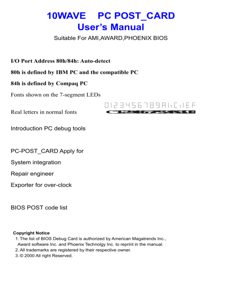
Fonts shown on the 7-segment LEDs
Real letters in normal fonts
0
1
2
3
4
5
6
7
8
9
A
B
C
D
E
F
Introduction PC debug tools
PC-POST_CARD Apply for
System integration
Repair engineer
Exporter for over-clock
BIOS POST code list
Copyright Notice
1. The list of BIOS Debug Card is authorized by American Magatrends Inc.,
Award software Inc. and Phoenix Technolgy Inc. to reprint in the manual.
2. All trademarks are registered by their respective owner.
3. © 2000 All right Reserved.
Introduction
Chapter 1
1-1 Introduction of PC debug tools
For motherboard debugging, we generally use the following tools except the Multi-Meter,
Oscilloscope, logic analyzer.
1. Debug Card (Port 80 card)
The primary function of Debug Card is to latch and display the BIOS POST code on card.
During system power on, the M/B perform the POST(Power On Self Test) routines. The main
purpose of these routines are to perform the diagnostics test upon the system component and
chipset initialization etc, The BIOS will put the POST code in the POST code port (for normal M/B
is Port 80h, and Compaq is 84h) before each respective task routine is performing.
When user plug the Debug Card into motherboard, we find the 2-digital 7-segment LED flash
display the different value on it. Each value present its respective routine of BIOS. If BIOS can’t
load the Operating System(O.S.) from disk diver, you will find the Debug Card stop and fixed
display the specific code on it. It is mean the BIOS can’t pass the program of POST. The user
can look up the BIOS POST lists of Appendix A to know function is defects. And rough to know
what kind problem occurs.
For the current Debug Card products, we find the PCI version are more public on the market.
Since the primary function of Debug Card is to display the POST code, we don’t need to consider
the performance for different bus slot. TO use the. ISA or PCI type POST card will get the same
result for POST code indicator. We only need to concern the point is the system support the bus
which can let POST card plug in or not. For PC 98 specification, the ISA is optional specification.
For PC 99, it suggests PC system PC system doesn’t support low speed ISA bus slot(We can
find the newer Intel chipset doesn’t have support supported the ISA specification). FOR PC
development trend, ISA will disappear soon that may be 1 or 2 years. In the above conclusion,
we know the PCI bus is primary extended bus in current PC architecture. So use PCI POST card
is best choice for purchasing.
THE POST card used for PC system assembly, motherboard test and BIOS debug.
2. Step By Step Card
The stet by step card used the hardware control to halt the CPU, then latch the address, data
and control signal on the card. The technician uses the card in working motherboard firstly, then
record the address, date and control signal result for each CPU halt step. For debugging stage,
technician dose same way and records the results that will be compare with working
motherboard’s result to find the defects. (This tools is useful to debug for address or data bus
problem).
These kinds products we can find a ISA or PCI. The step by step card used in the motherboard
debug for senior professional engineer.
1-2Introduction of POST card
POST card shows the POST code on board, t responses the current POST program status.
When POST code stop a fixed before boot the operating system, it is mean something problems
occurs, User can check the message of BIOS POST cod e lists of BIOS brand used in your
motherboard to know what problem occurs now.
1-2-1 Introduction of new PCI POST card
New generation PCI POST card is designed with the PCI bus core logic and ASIC technology. It
can work in any kind motherboard designs with PCI bus. (For the past simple GALs designed
version, it just pure designed the PORT 80/84 decoder, it can’t work in new motherboard
designed which method used to solve the EMI problem and reduce system power
dissipation . For this kind motherboard, if you used simple decode POST card, it will lose the
POST code readout function during POST testing.)
We create the new auto port 80/84 switch function in new generation PCI POST card. It can auto
switch to port 80 for general motherboard , switch to port 84 for Compaq motherboard after
system power on. In new generation designed, it will not display abnormal post code and real
perform abnormal post code and real perform the auto-switch between port 80 and 84.
PC-POST_CARD Specification
Fully compatible with any kind motherboard (80486, Pentium, Pentium Ⅱ , Pentium Ⅲ , P4
and AMD Athlon ) which has the PCI bus slot.
Auto port 80h/84h switch without jumper setting. It auto switches to port 80h for general
motherboard, to switch port 84h for Compaq motherboard after power on for POST function
execution.
Dual POST code display – User readout the POST at PCB component and solder side. It is
easy to view the POST code when user plug the POST card in computer system.
REAL PC I Step by Step Card
For 21 century, some new technology will replace the old one. The ISA bus of motherboard will
be disappear current. The debug technology and tools will be updated. (most of debug tools is
based on ISA bus). Some of PCI step by step is just only latch the address and data, it can not
stop and complex for operation to troubleshooting in the market.
Debug Instruction
POST code = FF,CPU can’t step
Check the power, RESET and their relative circuit. Refer the C/BE LED signal of PCI step
card to solve some CPU command fault problem.
POST code = FFF,CPU can step
The primary defect of this condition are address or data bus path signal problem. Used the
step by step card to record the address and data step by then compare the correct one to find the
defect.
POST CODE stop a fixed value
It represent the system can’t pass one of BIOS POST CODE check point to let M/B stop at
beginning of this POST test. Continue to step by step for IOR/W to record the result to compare a
god one to solve the problem.
Specification
.
1. Support step by step data latch function. It must connect reset to motherboard.( The card will
increase step automatically, it is full emulate the operating way same as ISA step by step card,
user didn’t learn any complex operating way for using new card.
2. Support the POST CODE display (Port 80h for general PC, 84h for Compaq PC)。
POST Card Usage
Chapter 2
How to install the POST card in the system ?
POST card is very easy to use for trouble-shooting, it just only plug the POST card into the
same type extend bus slot of motherboard.
Installation notice
1. Please be careful the direction of install the ISA type POST card(it is same way as general
way as general ISA card, the component in right side of PCB after plug into ISA bus), if plug
in wrong direction will damage the card.
2. Please don’t install the PCI POST into ISA bus slot, our FAE find little customer has this
mistake.(We think we ISA bus slot disappears, this problem will disappear for future new PC
architecture)
Trouble-shooting of using POST Card?
1. Plug the POST card in tested motherboard for same type expended slot.
2. Refer signal & power LED of POST card to solve these kinds problem firstly.
3. Get the POST code from card and check your motherboard BIOS brand to look up for BIOS
POST lists to error message for debug.
Protect your testing equipment
Help you saving Money
Protector : Protect the CPU, RAM Module, Motherboard, Add- On Card...etc. testing equipment
During the testing process, the engineers must insert/pull the CPU. RAM Module, Add - On Card ...
etc. Testing equipment many hundreds of times. There are easy broken during the testing
process.
Apply the POST card
Chapter 3
Applicant: System integrator
Question : When system power on, nothing show on monitor
Requirement: Identify the damage is resulted from Switch power supply, Motherboard, CPU,
RAM module, VGA card or monitor.
Verification step
1. Insert the right POST card into the extension slot the extension slot of PC motherboard to be
verify.
2. Turn on system, check POST card power indicators are all on or not . If not, check the power
core cable, power connector and power supply fan to solve the power problem firstly.
3. When system can’t boot the O.S. and POST card stopped at fixed POST code, please check
BIOS POST code list to know what kind problem occur.
Error cause by
CPU
BIOS POST message
CPU relative function check
Math
Coprocessor
Memory
Coprocessor relative
Function check
DRAM , refresh and
DRAM controller
relative function check
VGA and display card relative Check and clear the VGA slot and golden finger
function check
or replace the VGA card to retest again.
Other POST . messages
Call customer service for help or replace M/B
except above items description
Display card
M/B
Trouble-shooting
Replace CPU (type and speed must be same), if
You replace another type CPU, please setup the
correct CPU type setting(include voltage , ration,
FSB clock) before power on the system.
Replace NPU or replace the CPU if NPU in built
in CPU.
Check and clear the RAM module socket and
golden finger or replace the RAM module.
Applicant: Motherboard repair engineer
Question : Motherboard malfunction
Requirement: Identify the defect circuit
Verification step
1. Insert the right POST card into the extension slot of PC motherboard to be verify.
2. Turn on system, check power problem firstly.
3. When POST card stop in fixed code, check the BIOS POST code list to know which function
failure. Use the Oscilloscope to check the its relative circuit to find the bug.
4. If the POST code stop at“FF”,it mean the system BIOS can’t do anything We can’t get error
information from POST code lists. In the manufacture stage, above problem’s primary reason are
address or data line malfunction. (You must the step by step card or HDICE to solve this kind
problem.)
3-1 Apply for Over-specification
Some of PC exporter like to use he over-specification for CPU, RMA module or VGA card to
enhance the system performance and doesn’t charge any cost. The POST card can help this kind
exporter to identify the CPU, PAM or Display card problem quickly.
Why POST card can identify above problem quickly?
When system BIOS can’t pass the POST, it will spot at its respective program and POST card will
show the POST card will show the POST code to let user know what kind the problem occur. We
can make conclusion as following table to identify the CPU, DRAM or VGA card problem.
Error cause by
CPU
BIOS POST code message
POST code = FF or Stop at
CUP relative function Check
Trouble-shooting
Slow down the FSB clock or CPU frequency ratio
CPU to set lower CPU working clock to test
again.
(most of CPU FIXED CPU frequency
ration, user can change setting to
modify CPU working).
Memory
POST code stop at CARM,
Slow down the DRAM clock setting until system
Refresh and DRAM controller can pass the memory test.
relative function check
Display card
POST code stop at SVGA and Slow down the VGA card slot bus clock
Display card relative function (sometime you must slow down the CPY FSB
check
clock or change the BIOS setup to Do it).
Additional description of over CPU working clock
CPU working clock = CPU FSB clock * CPU frequency ratio
User can setup difference FSB clock or ratio to change the CPU clock. When user over too much
CPU clock, the system will do anything for BIOS, it will show the ‘‘FF’’ on the POST card.
In the over CPU clock experience, we can add more CPU cooler (such as high speed fan) to let
CPU working in higher speed. User can also increase the CPU VCORE voltage to let CPU
working in higher speed, but don’t increase too much otherwise it will damage the CPU parts.
(normal increase about 0.1 - 0.2V of original specification is save, User can change by jumper
setting or BIOS SETUP depend on different motherboard support it ). When user increase the
CPU speed, it will produce more hilt on CPU and system, you must improve the cooler system to
remain system reliability.
Additional description of over DRAM working clock
The memory cost gap is not same as CPU for different specification and difficult to enhance the
cooler system on the DRAM module , we suggest to use the real specification for DRAM work or
doesn’t over too mush clock frequency on it. For example:
SDRAM
specification
Over specification suggest
100 MHz
doesn’t more than 120 MHz
133 MHz
doesn’t more than 150 MHz
The above parameter is suggestion value, it depends on the SDRAM module maker.
User can adjust the SDRAM CAS latency clock to change SDRAM performance (CL-2 or CL-3,
user can change these parameter by BIOS SETUP, CL-2 is quicker than CL-3 mode)
How to distinguish CL=2 and CL=3 of DRAM module by POST card ?
1. Insert the POST card in motherboard.
2. Run the BIOS SERUP program for CL=2 and CL=3, and test for each condition. Please refer
the following table to get results.
CL=2 test CL=3 test SDRAM Module type & action
PASS
PASS
CL=2. Try to up the DRAM clock and test again, if you want to use this
module for more higher speed.
FAIL
PASS
CL=3 DRAM module.
FAIL
FAIL
Bad module, try to down the DRAM clock and test again to search a
working operating specification for this module.
BIOS POST code Lists
-----Appendix A
In the Appendix A section you may find the POST code lists message for AMI, Award and Phoenix
BIOS, you may refer the POST code show on POST card to Appendix A lists or the BIOS POST
list from your system supplier, and find out the defective parts. Following us the brief description or
relationship between the POST card, PC system and POST code, and how to benefit from the
POST code.
When system turns on, BIOS will initialize and verify every part of system, and test function, every
initialization, verification and test mean a small, separate program, and have its own POST code.
The POST code will be exported prior to execute the small program, if the initialization, verification
or test fails, system will pause and POST code will keep showing on the card, you may find out the
defective part by checking the meaning of the POST code. Now we can conclude as follows:
1. POST card: Show the system self-test status and POST code.
2. POST code: dedicated code for every small program of POST including initialization, verification
and test, the combination of every small program means Power On Self-Test(POST).
▓POST card is compatible with every IBM compatible system, since there are too many BIOS
supplier and the version changes soon, if you system BIOS information can’t find here, please
check ask the BIOS supplier for free information or download by their respective web site.
▓The BIOS code here may be called Error code, POST error code, Port 80 code in your system
manual.
All the BIOS POST code listings source are performed by the BIOS supplier (The
POST Messages
During the Power On Self-Test (POST), if the BIOS detects an error requiring you to do something
to fix, it will either sound a beep code or display a message.
If a message is displayed, it will be accompanied by:
PRESS F1 TO CONTINUE, CTRL-ALT-ESC OR DEL TO ENTER SETUP
POST Beep
Currently there are two kinds of beep codes in BIOS. This code indicates that a video error has
occurred and the BIOS cannot initialize the video screen to display any additional information.
This beep code consists of a single long beep followed by two short beeps. The other code
indicates that your DRAM error has occurred. This beep code consists of a single long beep
repeatedly.
Error Messages
One or more of the following messages may be displayed if the BIOS detects an error during the
POST. This list includes messages for both the ISA and the EISA BIOS.
CMOS BATTERY HAS FAILED
CMOS battery is no longer functional. It should be replaced.
CMOS CHECKSUM ERROR
Checksum of CMOS is incorrect. This can indicate that CMOS has become corrupt. This error
may have been caused by a weak battery. Check the battery and replace if necessary.
DISK BOOT FAILURE, INSERT SYSTEM DISK AND PRESS ENTER
No boot device was found. This could mean that either a boot drive was not detected or the drive
does not contain proper system boot files. Insert a system disk into Drive A: and press <Enter>.
If you assumed the system would boot from the hard drive, make sure the controller is inserted
correctly and all cables are properly attached. Also be sure the disk is formatted as a boot device.
Then reboot the system.
DISKETTE DRIVES OR TYPES MISMATCH ERROR - RUN SETUP
Type of diskette drive installed in the system is different from the CMOS definition. Run Setup to
reconfigure the drive type correctly.
DISPLAY SWITCH IS SET INCORRECTLY
Display switch on the motherboard can be set to either monochrome or color. This indicates the
switch is set to a different setting than indicated in Setup. Determine which setting is correct,
and then either turn off the system and change the jumper, or enter Setup and change the VIDEO
selection.
DISPLAY TYPE HAS CHANGED SINCE LAST BOOT
Since last powering off the system, the display adapter has been changed. You must configure
the system for the new display type.
EISA Configuration Checksum Error
PLEASE RUN EISA CONFIGURATION UTILITY
The EISA non-volatile RAM checksum is incorrect or cannot correctly read the EISA slot. This can
indicate either the EISA non-volatile memory has become corrupt or the slot has been configured
incorrectly. Also be sure the card is installed firmly in the slot.
EISA Configuration Is Not Complete
PLEASE RUN EISA CONFIGURATION UTILITY
The slot configuration information stored in the EISA non-volatile memory is incomplete.
Note: When either of these errors appear, the system will boot in ISA mode, which allows you to
run the EISA Configuration Utility.
ERROR ENCOUNTERED INITIALIZING HARD DRIVE
Hard drive cannot be initialized. Be sure the adapter is installed correctly and all cables are
correctly and firmly attached. Also be sure the correct hard drive type is selected in Setup.
ERROR INITIALIZING HARD DISK CONTROLLER
Cannot initialize controller. Make sure the cord is correctly and firmly installed in the bus. Be
sure the correct hard drive type is selected in Setup. Also check to see if any jumper needs to be
set correctly on the hard drive.
FLOPPY DISK CNTRLR ERROR OR NO CNTRLR PRESENT
Cannot find or initialize the floppy drive controller. make sure the controller is installed correctly
and firmly. If there are no floppy drives installed, be sure the Diskette Drive selection in Setup is
set to NONE.
Invalid EISA Configuration
PLEASE RUN EISA CONFIGURATION UTILITY
The non-volatile memory containing EISA configuration information was programmed incorrectly or
has become corrupt. Re-run EISA configuration utility to correctly program the memory.
NOTE: When this error appears, the system will boot in ISA mode, which allows you to run the
EISA Configuration Utility.
KEYBOARD ERROR OR NO KEYBOARD PRESENT
Cannot initialize the keyboard. Make sure the keyboard is attached correctly and no keys are
being pressed during the boot.
If you are purposely configuring the system without a keyboard, set the error halt condition in Setup
to HALT ON ALL, BUT KEYBOARD. This will cause the BIOS to ignore the missing keyboard and
continue the boot.
Memory Address Error at ...
Indicates a memory address error at a specific location. You can use this location along with the
memory map for your system to find and replace the bad memory chips.
Memory parity Error at ...
Indicates a memory parity error at a specific location. You can use this location along with the
memory map for your system to find and replace the bad memory chips.
MEMORY SIZE HAS CHANGED SINCE LAST BOOT
Memory has been added or removed since the last boot. In EISA mode use Configuration Utility to
reconfigure the memory configuration. In ISA mode enter Setup and enter the new memory size in
the memory fields.
Memory Verify Error at ...
Indicates an error verifying a value already written to memory. Use the location along with your
system's memory map to locate the bad chip.
OFFENDING ADDRESS NOT FOUND
This message is used in conjunction with the I/O CHANNEL CHECK and RAM PARITY ERROR
messages when the segment that has caused the problem cannot be isolated.
OFFENDING SEGMENT:
This message is used in conjunction with the I/O CHANNEL CHECK and RAM PARITY ERROR
messages when the segment that has caused the problem has been isolated.
PRESS A KEY TO REBOOT
This will be displayed at the bottom screen when an error occurs that requires you to reboot.
Press any key and the system will reboot.
PRESS F1 TO DISABLE NMI, F2 TO REBOOT
When BIOS detects a Non-maskable Interrupt condition during boot, this will allow you to disable
the NMI and continue to boot, or you can reboot the system with the NMI enabled.
RAM PARITY ERROR - CHECKING FOR SEGMENT ...
Indicates a parity error in Random Access Memory.
Should Be Empty But EISA Board Found
PLEASE RUN EISA CONFIGURATION UTILITY
A valid board ID was found in a slot that was configured as having no board ID.
NOTE; When this error appears, the system will boot in ISA mode, which allows you to run the
EISA Configuration Utility.
Should Have EISA Board But Not Found
PLEASE RUN EISA CONFIGURATION UTILITY
The board installed is not responding to the ID request, or no board ID has been found in the
indicated slot.
NOTE: When this error appears, the system will boot in ISA mode, which allows you to run the
EISA Configuration Utility.
Slot Not Empty
Indicates that a slot designated as empty by the EISA Configuration Utility actually contains a
board.
NOTE: When this error appears, the system will boot in ISA mode, which allows you to run the
EISA Configuration Utility.
SYSTEM HALTED, (CTRL-ALT-DEL) TO REBOOT ...
Indicates the present boot attempt has been aborted and the system must be rebooted. Press
and hold down the CTRL and ALT keys and press DEL.
Wrong Board In Slot
PLEASE RUN EISA CONFIGURATION UTILITY
The board ID does not match the ID stored in the EISA non-volatile memory.
NOTE: When this error appears, the system will boot in ISA mode, which allows you to run the
EISA Configuration Utility.
FLOPPY DISK(S) fail (80) Unable to reset floppy subsystem.
FLOPPY DISK(S) fail (40) Floppy Type dismatch.
Hard Disk(s) fail (80)
HDD reset failed
Hard Disk(s) fail (40)
HDD controller diagnostics failed.
Hard Disk(s) fail (20)
HDD initialization error.
Hard Disk(s) fail (10)
Unable to recalibrate fixed disk.
Hard Disk(s) fail (08)
Sector Verify failed.
Keyboard is locked out - Unlock the key.
BIOS detect the keyboard is locked. P17 of keyboard controller is pulled low.
Keyboard error or no keyboard present.
Cannot initialize the keyboard. Make sure the keyboard is attached correctly and no keys are
being pressed during the boot.
Manufacturing POST loop.
System will repeat POST procedure infinitely while the P15 of keyboard controller is pull low. This
is also used for M/B burn in test.
BIOS ROM checksum error - System halted.
The checksum of ROM address F0000H-FFFFFH is bad.
Memory test fail.
BIOS reports the memory test fail if the onboard memory is tested error.
AMI BIOS POST Code Listing v6.2.4
POST Code
D0
D1
D3
D4
D5
D6
D7
D8
D9
AMI WinBIOS uncompress code checkpoints Description
NMI is Disabled. CPU ID saved. Init code Checksum verification starting.
To do DMA init, keyboard controller BAT test, start memory refresh and going to
4Gbflat mode.
TO start memory sizing.
TO comeback to real mode. Execute OEM patch. Set stack.
E000 ROM enabled. Init code is copied to segment 0 and control to be transferred to
segment 0.
Control is in segment 0.To check<CTRL><HOME>key and verify main BIOS
checksum. IF either <CTRL><HOME>is pressed or main IOS checksum is bad, go to
check point E0 else go to check point D7.
To pass control to Interface Module.
Main BIOS runtime code is to be decompressed.
Control to be passed to main BIOS in shadow RAM.
Runtime code is uncompressed in F000 shadow ram
POST Code AMI HiFLEX BIOS/WinBIOS runtime code Description
E0
Onboard floppy controller (if any) is initialzed. To start base 512K memory test.
E1
To initialize interrupt vector table.
E2
To initialize DMA and interrupt controllers.
E6
To enable floppy and timer IRQ, enable internal cache.
ED
Initialize floppy drive.
EE
Start looking for diskette in drive A: and read 1st sector of the diskette.
EF
Floppy read error.
F0
Start searching ‘AMIBOOT.ROM’ file in root directory.
F1
MIBOOT.ROM’ file not present in root directory.
F2
Start reading FAT table and analyze FAT to find the clusters occupied by
MIBOOT.ROM’ file..
F3
Start reading MIBOOT.ROM’ file cluster by cluster.
F4
MIBOOT.ROM’ file not of proper size.
F
Disable internal cache.
FB
Detect flash type present.
FC
Erase flash.
FD
Program flash.
FF
Flash Program successful BIOS is going to restart Runtime code is uncompressed in
F000 shadow ram.
03
Power on delay complete. To check soft rest/power-on.
05
Soft reset/power-on determined. Going to disable Cache if any.
06
POST code to be uncompressed.
07
POST code is uncompressed. CPU init and CPU data area init to be
done next
08
CPU and CPU data area init done. CMOS checksum calculation to be
done next.
0B
CMOS status register init done.
Any initialization before keyboard BAT to be done next.
0C
KB controller I/B free. Going to issue the BAT command to keyboard
Controller.
0E
Keyboard controller BAT result verified.
Any initialization after KB controller BAT to be done next.
0F
Initialization after KB controller BAT done.
10
11
12
13
14
19
1A
20
23
24
25
27
28
2A
2B
2C
2D
2E
2F
30
31
32
34
37
38
39
3A
40
42
43
44
45
46
Keyboard command byte to be written next.
Keyboard controller command byte is written.
Going to issue Pin-23 ,24 blocking/unblocking command.
Pin-23,24 of keyboard controller is blocked/ unblocked.
Going to check pressing of <INS><END> key during power-on.
Checking for pressing of <END> key during power-on done.
Going to disable DMA and Interrupt controllers.
DMA controller #1,#2, interrupt controller #1,#2 disabled.
Video display is disabled and port-B is initialized. Chipset init about to
Begin.
8254 timer test about start.
8254 timer test over . About to start memory refresh test.
Memory Refresh line is togging . going to check15 micro second ON/OFF
Memory Refresh period 30 micro second test complete.
Base 64K memory to be initialized.
To read 8042 input port and disable Megakey Green PC feature. Make bios code
segment writeable.
To do any setup before Int vector init.
Interrupt vector initialization done. Going to read Input port of 8042 for turbo switch (of
any ) and to clear password if post diag switch is on.
Any initialization before setting video mode to be done next.
Initialization before setting video mode is complete.
Going for monochrome mode and color mode setting.
Different BUSes init (system, static, output devices ) to start if present.
(Please see next section for details of different BUSes).
About to give control for any setup required before optional video ROM check.
Processing before video ROM control is done.
About to look for optional video ROM and give control.
Optional video ROM control is done.
About to give control to do any processing after video ROM returns control.
Return from processing after the video ROM control.
If EGA/VGA not found then do display memory R//w test.
EGA/VGA not found. Display memory R/W test about to begin.
Display memory R/W test passed. About to look for the retrace checking.
Display memory R/W test or retrace checking failed.
About to do alternate Display memory R/W test.
Alternate Display memory R/W test passed.
About to look for the alternate display retrace checking.
Video display checking over. Display mode to be set next.
Display mode set. Going to display the power on message.
Different BUSes init (input, IPL, general devices)to start if present.
(Please see next section for details of different BUSes).
Display different BUSes initialization error messages.
(Please see Appendix for details of different BUSes).
New cursor position read and saved. Going to display the Hit <DEL> message.
Going to prepare the descriptor tables.
Descriptor tables prepared. Going to enter in virtual mode for memory test.
Entered in the virtual mode. Going to enable interrupts for diagnostics mode.
Interrupts enabled (if diagnostics switch is on).
Data initialized. Going to check for memory wrap around at 0:0 and finding the total
system memory size.
Memory wrap around test done. Memory size calculation over.
About to go for writing patterns to test memory.
47
48
49
4B
4C
4D
4E
4F
50
51
52
53
54
57
58
59
60
62
65
66
67
7F
80
81
82
83
84
85
86
87
88
89
8B
Pattern to be tested written in extended memory.
Going to write patterns in base 640k memory.
Patterns written in base memory.
Going to find out amount of memory below 1M memory.
Amount of memory below 1M found and verified.
Going to find out amount of memory above 1M memory.
Amount of memory above 1M found and verified. Check for soft reset and going to
clear memory below 1M memory.
Memory below 1M cleared.(SOFT RESET) Going to clear memory above 1M.
Memory above 1M cleared.(SOFT RESET)
Going to save the memory size. (Go to check point# 52h).
Memory test started. (NOT SOFT RESET)About to display the first 64k memory size.
Memory size display started. This will be updated during memory test.
Going for sequential and random memory test.
Memory testing/initialization below 1M complete.
Going to adjust displayed memory size for relocation/ shadow.
Memory size display adjusted due to relocation/ shadow.
Memory test above 1M to follow.
Memory testing/initialization above 1M complete
Going to save memory size information.
Memory size information is saved. CPU registers are saved.
Going to enter in real mode.
Shutdown successful, CPU in real mode.
Going to disable gate A20 line and disable parity/NMI.
A20 address line, parity/NMI disable successful.
Going to adjust memory size depending on relocation/shadow.
Memory size adjusted for relocation/shadow. Going to clear Hit <DEL> message.
Hit <DEL> message cleared. <WAIT…>message displayed.
About to start DMA and interrupt controller test.
DMA page register test passed. To do DMA#1 base register test.
DMA#1 base register test passed. To do DMA#2 base register test.
DMA#2 base register test passed. TO program DMA unit 1and 2.
DMA unit 1 and 2 programming over. To initialize 8259 interrupt controller.
8259 /initialization over.
Extended NMI sources enabling is in progress.
Keyboard test started. Clearing output buffer, checking for stuck key, About to issue
keyboard reset command,
Keyboard reset error/stuck key found.
About to issue keyboard controller interface test command.
Keyboard controller interface test over.
About to write command byte and init circular buffer.
Command byte written, Global date init done. About to check for lock-key.
Lock-key checking over. About to check for memory size mismatch with CMOS.
Memory size check done.
About to display soft error and check for password or bypass setup.
Password checked About to do programming before setup.
Programming before setup complete.
Going to uncompress SETUP code and execute CMOS setup.
Returned from CMOS setup program and screen is cleared.
About to do programming after setup.
Programming after setup complete. Going to display power on screen message.
First screen message displayed <WAIT…>message displayed.
About to do Video BIOS shadow.
8C
8D
8F
91
95
96
97
98
99
9A
9B
9C
9D
9E
A2
A3
A4
A5
A7
A8
A9
AA
AB
AC
B0
B1
00
Video BIPS shadow successful.
Setup options programming after CMOS setup about to start.
Going for hard disk controller reset.
Hard disk controller reset done. Floppy setup to be done next.
Floppy setup complete. Hard disk setup to be done next.
Memory size adjusted due to mouse support. Init of different BUSes optional ROMs
from C800 to start. (Please see next section for details of different BUSes).
Going to do any init before C800 optional ROM control.
Any init before C800 optional ROM control is over.
Optional ROM check and control will be done next.
Optional ROM control is done. About to give control to do any required processing
after optional ROM returns control.
Any initialization required after optional ROM test over.
Going to setup timer data area and printer base address.
Return after setting timer and printer base address.
Going to set the RS-323 base address.
Returned after RS-323 base address.
Going to do any initialization before Coprocessor test.
Required initialization before Coprocessor is over.
Going to initialize the Coprocessor next.
Coprocessor initialized. Going to do any initialization after Coprocessor test.
Initialization after Coprocessor test is complete.
Going to check extd keyboard, keyboard ID and num-lock.
Cache memory test over. Going to display any soft errors.
Soft error display complete. Going to set keyboard typematic rate.
Keyboard typematic rate set. To program memory wait states.
Memory wait states programming over.
Going to clear the screen and enable parity/NMI.
NMI and parity enabled.
Going to do any initialization required before giving control to optional ROM at E000.
Initialization before E000 ROM control over . E000 ROM to get control next.
Returned from E000 ROM control.
Going to do any initialization required after E000 optional ROM control.
Initialization after E000 optional ROM control is over.
Going to display the system configuration.
To build mp table if needed.
To uncompress DMI data and execute DMI POST init.
System configuration is displayed.
Going to copy any code to specific area.
Copying of code to specific area done. Going to give control to INT-19 boot loader.
For more information about AMI BIOS please refer to the Award website at http://www.ami.com.tw/
AWARD BIOS POST Code Listing v6.0
POST (hex)
CFh
C0h
C1h
C3h
C5h
01h
02h
03h
04h
05h
06h
07h
08h
09h
0Ah
0Ch
0Dh
0Eh
0Fh
10h
11h
12h
13h
14h
15h
16h
17h
18h
19h
1Ah
Description
Test CMOS R/W functionality.
Early chipset initialization:
-Disable shadow RAM
-Disable L2 cache (socket 7 or below)
-Program basic chipset registers
Detect memory
-Auto-detection of DRAM size, type and ECC.
-Auto-detection of L2 cache (socket 7 or below)
Expand compressed BIOS code to DRAM
Call chipset hook to copy BIOS back to E000 & F000 shadow
RAM.
Expand the Xgroup codes locating in physical address 1000:0
Reserved
Initial Superio_Early_Init switch.
Reserved
1. Blank out screen
2. Clear CMOS error flag
Reserved
1. Clear 8042 interface
2. Initialize 8042 self-test
1. Test special keyboard controller for Winbond 977 series Super
I/O chips.
2. Enable keyboard interface.
Reserved
1. Disable PS/2 mouse interface (optional).
2. Auto detect ports for keyboard & mouse followed by a port & interface swap
(optional).
3. Reset keyboard for Winbond 977 series Super I/O chips.
Reserved
Reserved
Test F000h segment shadow to see whether it is R/W-able or not. If
test fails, keep beeping the speaker.
Reserved
Auto detect flash type to load appropriate flash R/W codes into the
run time area in F000 for ESCD & DMI support.
Reserved
Use walking 1’s algorithm to check out interface in CMOS
circuitry. Also set real-time clock power status, and then check
for override.
Reserved
Program chipset default values into chipset. Chipset default
values are MODBINable by OEM customers.
Reserved
Initial onboard clock generator if Early_Init_Onboard_Generator
is defined. See also POST 26h.
Reserved
Detect CPU information including brand, SMI type (Cyrix or
Intel) and CPU level (586 or 686).
Reserved
Reserved
POST (hex)
1Bh
1Ch
1Dh
1Eh
1Fh
20h
21h
22h
23h
24h
25h
26h
27h
28h
29h
2Ah
2Bh
2Ch
2Dh
2Eh
2Fh
30h
31h
32h
33h
34h
35h
36h
37h
38h
39h
3Ah
Description
Initial interrupts vector table. If no special specified, all H/W
interrupts are directed to SPURIOUS_INT_HDLR & S/W
interrupts to SPURIOUS_soft_HDLR.
Reserved
Initial EARLY_PM_INIT switch.
Reserved
Load keyboard matrix (notebook platform)
Reserved
HPM initialization (notebook platform)
Reserved
1.Check validity of RTC value:
e.g. a value of 5Ah is an invalid value for RTC minute.
2. Load CMOS settings into BIOS stack. If CMOS checksum fails, use default value
instead.3. Prepare BIOS resource map for PCI & PnP use.If ESCD is valid,
take into consideration of the ESCD’s legacy information.4.onboard clock generator
initialization. Disable respective clock resource to empty PIC&DIMM slots.
5.Early PCI Initialization:
-Enumerate PCI bus number.
-Assign memory & I/O resource
-Search for a valid VGA device & VGA BIOS, and put it into
C000:0
Reserved
Reserved
Reserved
Initialize INT 09 buffer
Reserved
1. Program CPU internal MTRR (P6 & PII) for 0-640K memory address.
2. Initialize the APIC for Pentium class CPU.
3. Program early chipset according to CMOS setup. Example: onboard IDE
controller.
4. Measure CPU speed.
5. Invoke Video BIOS.
Reserved
Reserved
Reserved
1. Initialize double-byte language font (Optional)
2. Put information on screen display, including Award title, CPU type, CPU speed, full
screen logo.
Reserved
Reserved
Reserved
Reserved
Reserved
Reset keyboard if Early_Reset_KB is defined e.g. Winbond 977
series Super I/O chips. See also POST 63h.
Reserved
Reserved
Reserved
Reserved
Reserved
Reserved
Reserved
POST (hex)
3Bh
3Ch
3Dh
3Eh
3Fh
40h
41h
42h
43h
44h
45h
46h
47h
48h
49h
4Ah
4Bh
4Ch
4Dh
4Eh
4Fh
50h
51h
52h
53h
54h
55h
56h
57h
58h
59h
5Ah
5Bh
5Ch
5Dh
5Eh
5Fh
60h
61h
62h
63h
Description
Reserved
Test 8254
Reserved
Test 8259 interrupt mask bits for channel 1.
Reserved
Test 8259 interrupt mask bits for channel 2.
Reserved
Reserved
Test 8259 functionality.
Reserved
Reserved
Reserved
Initialize EISA slot
Reserved
1. Calculate total memory by testing the last double word of each 64K page.
2. Program write allocation for AMD K5 CPU.
Reserved
Reserved
Reserved
Reserved
1. Program MTRR of M1 CPU
2. Initialize L2 cache for P6 class CPU & program CPU with proper cacheable range.
3. Initialize the APIC for P6 class CPU.
4. On MP platform, adjust the cacheable range to smaller one in case the cacheable
ranges between each CPU are not identical.
Reserved
Initialize USB.
Reserved
Test all memory (clear all extended memory to 0)
Reserved
Reserved
Display number of processors (multi-processor platform)
Reserved
1. Display PnP logo
2. Early ISA PnP initialization
-Assign CSN to every ISA PnP device.
Reserved
Initialize the combined Trend Anti-Virus code.
Reserved
(Optional Feature)
Show message for entering AWDFLASH.EXE from FDD
(optional)
Reserved
1. Initialize Init_Onboard_Super_IO
2. Initialize Init_Onbaord_AUDIO.
Reserved
Reserved
Okay to enter Setup utility; i.e. not until this POST stage can users
enter the CMOS setup utility.
Reserved
Reserved
Reserved
POST (hex)
64h
65h
66h
67h
68h
69h
6Ah
6Bh
6Ch
6Dh
6Eh
6Fh
70h
71h
72h
73h
74h
75h
76h
77h
78h
79h
7Ah
7Bh
7Ch
7Dh
7Eh
7Fh
80h
81h
82h
83h
84h
85h
Description
Reserved
Initialize PS/2 Mouse
Reserved
Prepare memory size information for function call:
INT 15h ax=E820h
Reserved
Turn on L2 cache
Reserved
Program chipset registers according to items described in Setup &
Auto-configuration table.
Reserved
1. Assign resources to all ISA PnP devices.
2. Auto assign ports to onboard COM ports if the corresponding item in Setup is set
to “AUTO”.
Reserved
1. Initialize floppy controller
2. Set up floppy related fields in 40:hardware.
Reserved
Reserved
Reserved
(Optional Feature)
Enter AWDFLASH.EXE if:
-AWDFLASH.EXE is found in floppy drive.
-ALT+F2 is pressed.
Reserved
Detect & install all IDE devices: HDD, LS120, ZIP, CDROM…..
Reserved
Detect serial ports & parallel ports.
Reserved
Reserved
Detect & install co-processor
Reserved
Init HDD write protect.
Reserved
Reserved
Switch back to text mode if full screen logo is supported.
-If errors occur, report errors & wait for keys
-If no errors occur or F1 key is pressed to continue:
Clear EPA or customization logo.
Reserved
Reserved
E8POST.ASM starts
1. Call chipset power management hook.
2. Recover the text fond used by EPA logo (not for full screen logo)
3. If password is set, ask for password.
Save all data in stack back to CMOS
Initialize ISA PnP boot devices
1. USB final Initialization
2. NET PC: Build SYSID Structure.
3. Switch screen back to text mode
4. Set up ACPI table at top of the memory.
5. Invoke all ISA adapter ROMs
POST (hex)
Description
6. Assign IRQs to PCI devices
7. Initialization APM
8. Clear noise of IRQs
86h
87h
88h
89h
90h
91h
92h
93h
94h
95h
96h
FFh
Reserved
Reserved
Reserved
Reserved
Reserved
Reserved
Reserved
Read HDD boot sector information for Trend Anti-Virus code
1. Enable L2 cache
2. Program boot up speed
3. Chipset final initialization.
4. Power management final initialization
5. Clear screen & display summary table
6. Program K6 write allocation
7. Program P6 class write combining
1. program daylight saving
2. Update keyboard LED & typematic rate
1. Build MP table
2. Build & update ESCD
3. Set CMOS century to 20h or 19h
4. Load CMOS time into DOS timer tick
5. Build MSIRQ routing table.
Boot attempt (INT 19h)
For more information about award BIOS please refer to the Award website at
http://www.award.com.tw/
Pheonix BIOS POST Code Listing
POST Code
02
04
06
08
09
0A
0C
0E
0F
10
11
12
14
16
18
1A
20
22
24
28
2A
2C
2E
32
34
35
37
38
39
3A
3C
3D
40
42
44
46
47
48
49
4A
4C
4E
POST Code
50
Phoenix POST Rountine Description
Verify Real Mode
Get CPU type
Initialize system hardware
Initialize chipset register with initial POST values
Set in POST flag
Initialize CPU register
Initialize cache to initial POST values
Initialize 1/0 CPU register
Initialize the local bus IDE
Initialize Power Management
Load alternate registers with initial POST values
Jump to UserPatch0
Initialize keyboard controller
BIOS ROM checksum
8254 timer initialization
8237 DMA controller initialization
Test DRAM refresh
Test 8042 keyboard controller
Set ES segment register to 4 GB
Autosize DRAM
Clear 512K base RAM
Test 512K base address lines
Test 512K base memory
Test CPU bus-clock frequency
Test CMOS RAM
Initialize alternate chipset registers
Reinitialize the chipset
Shawdow system BIOS ROM
Reinitialize the cache
Autosize cache
Configure advanced chipset registers
Load alternate registers with CMOS values
Set initial CPU aped
Initialize interrupt vectors
Initialize BIOS interrupts
Check ROM copyright notice
Initialize manager for PCI Option ROMs
Check video configuration against CMOS
Initialize PCI bus and devices
Initialize all video adapters in system
Shadow video BIOS ROM
Display copyright notice
Phoenix POST Rountine Description
Display CPU type and speed
51
52
54
56
58
5A
5C
60
62
64
66
68
6A
6C
6E
70
72
74
76
7C
7E
80
82
84
86
88
8A
8C
90
91
92
93
94
96
98
9A
9C
9E
A0
A2
A4
A8
AA
POST Code
AC
Initialize EISA board
Test keyboard
Set key click if enabled
Enable keyboard
Test for unexpected interrupts
Display prompt ”Press F2 to enter SETUP”
Test RAM between 512to 640K
Test extended memory
Test extended memory address lines
Jump to UserPatsh1
Configure advanced cache registers
Enable external and CPU cache
Display external cache size
Display shadow message
Display non-disposable segments
Display error messages
Check for configuration errors
Test real-time clock
Check for keyboard errors
Setup hardware interrupt vectors
Test corprocessor if presents
Disable onboard I/O ports
Detect and install external RS-232 ports
Detect and install external parallel ports
Re-initialize onboard I/O ports
Initialize BIOS Data Area
Initialize Extended BIOS Data Area
Initialize floppy controller
Initialize hard-disk controller
Initialize local-bus hard-disk controller
Jump to UserPatch2
Built MPTABLE for multi-processor boards
Disable A20 address line
Clear huge ES segment register
Search for option ROMs
Shadow option ROMs
Set up Power Management
Enable hardware interrupts
Set time of day
Check key lock
Initialize typematic rate
Ease F2 prompt
Scan for F2 stroke
Phoenix POST Rountine Description
Enter SETUP
AE
B2
B4
B6
B8
BC
BE
BF
C0
D0
D2
D4
D6
D8
DA
DC
Clear in-POST flag
POST done-prepare to boot operating system
One beep
Check password (option)
Clear global descriptor table
Clear parity checkers
Clear screen (option)
Clear virus and backup remainders
Try to boot with INT19
Interrupt handler error
Unknown interrupt error
Pending interrupt error
Initialize option ROM error
Shutdown error
Extended BLOCK Move
Shutdown 10 error
For more information about Phoenix BIOS please refer to the Phoenix website at http://www.phoenix.com
