Semi-Dynamic and Dynamic Flip-FLops with Embedded
advertisement
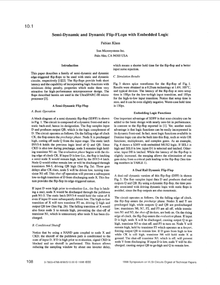
10.1 Semi-Dynamic and Dynamic Flip-FLops with Embedded Logic Fabian mass Sun Microsystems Inc. Palo Alto, CA 94303 USA In troductioii This paper describes a family of semi-dynamic and dynamic edge-triggered flip-flops to be used with static and dynamic circuits, respectively [1][2]. The flip-flops provide both short latency and the capability of incorporating logic functions with minimum delay penalty, properties which make them very attractive for high-performance microprocessor design. The flops described herein are used in the UltraSPARC-III microprocessor [3]. A Semi-Dynamic Flip-Flop A. Basic Operation A block diagram of a semi-dynamic flip-flop (SDFF) is shown in Fig. 1. The circuit is composed of a dynamic front-end and a static backend. hence its designation. The flop samples input D and produces output QB, which is the logic complement of D. The circuit operates as follows. On the falling edge of clock CK,the flop enters the preclzarge phase. Node X is precharged high, cutting off node Q from the input stage. The static latch INV5-6 holds the previous logic level of Q and QB. Since CKD is also low during precharge, node S remains high holding transistor N 1 on. The evaluation phase begins with the rising edge of clock CX.If input D is low (i.e., the flop is latching a zero) node X would remain high, held by the INV3-4 latch. Node Q would either remain law or will be discharged through transistors N4-5, driving QB high (See Fig. 2a). Three gate delays after CK rises, node S will be driven low, turning transistor N1 off. This shut-ofoperation will prevent a subsequent low-to-high transition of D from discharging node X. This feature provides the flip-flop its edge-triggered nature. If input D were high prior to evaluation (i.e., the flop is latching a one), node X would be discharged through the pulldown path N1-3. The static latch INV3-4 would hold the value of X even if input D were subsequently driven low.The high-to-low transition of X will turn transistor €9on, driving Q high and output QB low (See Fig. 2b). The falling transition of X would also force node S to remain high, preventing the shut-off of transistor N1, which is unnecessary after node X has been discharged. B. Conditional Shutoff Notice that by using a NAND gate coupled to node X and CKD, the shutoff of the pulldown path is conditioned to the state of input D. If D is high prior to evaluation, signal CKD is blocked and no shutoff is performed. This feature allows reducing the sampling window by about one inverter delay, 108 0-7803-4766-8/98/$10.00 0 1998 IEEE which means a shorter hold time for the flip-flop and a better input noise rejection. C. Simulation Results Fig. 3 shows spice waveforms for the flip-flop of Fig. 1. Results were obtained in a 0 . 2 5 technology ~ at 1.6V. 10SoC, and typical devices. The latency of the flip-flop at zero setup time is 188ps for the low-to-high input transition, and 185ps for the high-to-low input transition. Notice that setup time is zero, and it can be even slightly negative. Worst-case hold time is 13qPs. Embedding Logic Functions One important advantage of SDFF is that scan circuitry can be added to the basic design with nearly zero hit in performance, in contrast to the flip-flop reported in 111. Yet. another main advantage is that logic functions can be easily incorporated in its dynamic front-end. In fact, most logic functions available in Domino logic can also be built into this flop, such as wide OR functions, multiplexors, and complex gates. As an example, Fig. 4 shows a SDFF with embedded MUX2 logic. If SELl is high and SELO is low, input D l is selected and latched. Otherwise, input DO is latched. While the latency of the flip-flop is slightly increased. the merging allows the elimination of one gate delay from a critical path leading to the flip-flop ( S e e timing numbers in TABLE 1). A Dual Rail Dynamic Flip-Flop A dual-rail dynamic version of this flip-flop (DFF) is shown Fig. 5. The f l o ~samples input data D and produces dual-rail outputs Q and QB. By using a dynamic flip-flop. the time penalty associated with driving dynamic logic with static flops is avoided. since the flop outputs are also monotonic. The circuit operates as follows. On the falling edge of clock. the flip-flop enters the precharge phase. Nodes X and Y are precharged high, while outputs Q and QB are predischarged low; transistors N6, N7, E,and P3 m all off, while transistors N1 and N3, the shut-ofdevices, are both on.On the rising edge ofclock, the flip-flop enters the evaluation phase. If input D is high, node X will be discharged, causing output Q to go high, transistor N3 to shut off. and P3 to turn on. Node Y will remain high, held by transistor P3 which operates as a keeper, forcing output QB to remain low. If D goes from high to low while CK is still high, transistor N6 will hold node X at ground. The shut-off transistor N3, which is off. will prevent node Y from discharging. If input D is low. node Y will be discharged. causing output QB to go high and Q to remain low. 1998 Symposium on VLSl Circuits Digest of Technical Papers The purpose of inverters INV2-3 and INV4-5 is to reduce the the flip-flop load on the critical nodes X and Y.This ”izes latency at the expense of a larger hold time. Similarly to SDFF, DFF can also incorporate logic functions. As an example, Fig. 6 shows a DFF with embedded MUX2 logic. Table 1 provides a sununary of the speed characteristics of the flip-flops discussed in i b i s paper. This includes: SDFF (Fig. 1). MuX2-SDFF (Fig. 4). SFF. which is a conventional pseudostatic master-slave flip-flop [4] using transmission gates and week feedback inverters, and SFF + static MUX2 gate (not shown). Compared to SFF. SDFF is about 33% faster. In addition,SDFF is about hadf the size, presents half the clock load, and requires a single clock phase. Fig. 3. Spice waveforms for SDFF Conclusion This paper describes it family of semi-dynamic and dynamic edge-biggered flip-flqx which are part of the UtraSPARC-111 miaoprocessor. They provide short latency, reduced clock load, a good interface to static and dynamic logic, and can easily incorporate logic fwtions with minimum delay penalty, eliminating one gate delay from a critical path. These flip-flops have played an integral roll in meeting the UltraSPARC-III cycle time goal. .:+ Fig. 4. SDFF with embedded MUX2 logic (MUXZSDFF) References T T H.Partovi, et al., “Flow-through latch and edge-triggered flip-flop hybrid elements,” ISSCC Digest of Technical Papers, pp. 132139,February 1996. N.B. Gaddis, J. R. 13utler, A. Kumar, W.J. Queen, “A 56-entry instruction reorder buffer,” ISSCC Digest of Technical Papers, pp. 212-213,February 1996. G. Lauterbach, “UltraSPARC-III an ultra-high clock rate SPARC for scalable systems,”Microprocessor Forum, San Jose, CA, October 1997. J. M. Rabaey, Digital Integrated Circuits: A Design Perspective, Prentice Hall,1996,pp. 349-350. T T CKF Q QB D CK +5 v Fig. 5. Edgetriggered T dynamic flipflop <~m -- I at- Q QB D1 -+@- w Fig. 1. Edge-triggered sed-dynamic flip-flop (SDFF) (a) Latching a zero Fig. 6. DIT with embedded MUX2 logic (MUX2-DFF) Q TABLE 1. Speed Comparisonof SDFF versus SFF QB I I Flip-Flop ’Qpe SDFF (b) Latching a one Q QB Fig. 2. Timing diagram bor SDFF t I Latency Speedup SFF 188PS 30Ops 1.6 1.o MUX2-SDFF 23Ops MUX2+SFF 48Ops 2.1 1.o 1998 Symposium on VLSl Circuits Digest of Technical Papers 109
