LAB 0 Introduction to Quartus II Software Design
advertisement
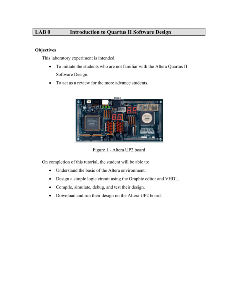
LAB 0 Introduction to Quartus II Software Design Objectives This laboratory experiment is intended: • To initiate the students who are not familiar with the Altera Quartus II Software Design. • To act as a review for the more advance students. Figure 1 - Altera UP2 board On completion of this tutorial, the student will be able to: • Understand the basic of the Altera environment. • Design a simple logic circuit using the Graphic editor and VHDL. • Compile, simulate, debug, and test their design. • Download and run their design on the Altera UP2 board. Background: The UP2 Education Board is a stand-alone experiment board based on a FLEX® 10K device and includes a MAX® 7000 device. When used with the Quartus II software, the board provides a superior platform for learning digital logic design using industrystandard development tools and PLDs. This board is designed specifically to meet the needs of instructors and students in a laboratory environment. The UP2 Education Board supports both look-up table (LUT) -based and product term-based architectures. The EPF10K70 device can be configured in-system with the ByteBlaster II download cable. The EPF10K70 device is based on SRAM technology. It is available in a 240-pin RQFP package and has 3,744 logic elements (LEs) and nine embedded array blocks (EABs). Each LE consists of a four-input LUT, a programmable flip-flop, and dedicated signal paths for carry-and-cascade functions. Each EAB provides 2,048 bits of memory which can be used to create RAM, ROM, or first-in first-out (FIFO) functions. EABs can also implement logic functions, such as multipliers, microcontrollers, state machines, and digital signal processing (DSP) functions. With 70,000 typical gates, the EPF10K70 device is ideal for intermediate to advanced digital design courses, including computer architecture, communications, and DSP applications. Laboratory In this tutorial, we will implement a simple circuit as shown below with AND, NAND and NOR functions to provide an introduction to the Altera Quartus II software. Figure 2 - A simple circuit with AND, NAND and NOR gates Part 1 - Design Entry Using schematic Capture Step 1 A. Design Using the Graphic Editor 1. Start Quartus II software. Choose FileÆ New Project Wizard. In the new window select Next, then in the next window set your desired working directory (Create a new directory called lab1p1) then choose lab1p1 (laboratory 1, part 1) for your file name and top-level design entity. Press Next. 2. We have no existing files, so in the new window click Next. 3. We will not use any third-part CAD tools, so in the new window press Next. 4. In the next window choose FLEX10K as target device family (make sure Yes is selected). Press Next. 5. In the list of available devices choose EPF10K70RC240-4 and press Next then Finish. B. Creating the Schematic 1. Select FileÆ New. A window appears that allows you to choose the type of file that should be created. Choose Block Diagram/Schematic File and click OK. An empty Block Editor window will appear. 2. Double click on the blank space inside the Block Editor display to open the directory labelled Libraries which lists several available libraries including Primitives library. Expand the directories to find a list of the Logic gates available in the Primitive library. 3. Scroll down in the Symbol Files box and double click on nor2. The symbol should appear in the center of the Graphic Editor. 4. Repeat step 1 and 2 and select a nand2 symbol. 5. Repeat step 1 and 2 again and select an and2 symbol. C. Assigning Output and Input pin 1. Open the Primitives Library again. 2. Scroll down past the gates until you reach pins. 3. Double click on Output. The symbol should appear on the Graphic Editor. 4. Repeat step 1 and 2 and select an Input symbol. 5. With the right mouse button copy and paste three more Input symbol. D. Connecting the Symbol 1. Go to the end of a symbol with the mouse and when the cross-symbol cursor appears drag the wire to the point to connect to, see diagram below for the connection. 2. Repeat the previous step for all connections. 3. If a wire is not properly run, just select it (wire turns red) and hit delete to remove it. 4. If you have problem running the wire from one point completely to another, try running half way from both devices. Also you can zoom in and out at any time. 5. The mouse can also be used to move a wire to the desired position. 6. Now, your diagram should look like the one below. 5 PIN_NAME INPUT VCC 6 PIN_NAME INPUT VCC NOR2 1 AND2 OUTPUT 4 3 7 PIN_NAME INPUT VCC 8 PIN_NAME INPUT VCC PIN_NAME NAND2 2 Figure 3 - Schematic with input and output wired E. Editing Pin Names 1. Double click on the pin_name1 on your first input symbol to select it. 2. Rename the pin as shown below. 3. Repeat for all input and output pins. 5 A INPUT VCC 6 B INPUT VCC NOR2 1 AND2 3 7 C INPUT VCC 8 D INPUT VCC NAND2 2 Figure 4 - Schematic Ports Name OUTPUT 4 Y F. Assign PIN Numbers 1. From Quartus II main menu choose AssignmentsÆ Assign Pins. 2. Choose pin number 28, Enter pin name, A and press Add. 3. Repeat steps 1 and 2 for pin numbers 29, 41, and 40 for pin names B, C, and D. See table below for all the necessary information. 4. Repeat the same steps for pin number 14 and output pin Y, but choose As output driving an unspecified signal instead of default As input tri-stated. 5. Press OK when finished. 6. Save your work. Pin Name Pin Number Pin Type A 28 Input tri-stated B 29 Input tri-stated C 41 Input tri-stated D 40 Input tri-stated Y 14 output driving an unspecified signal Location On the board Pushbutton 1 (non-debounced, 0 = button pressed) Pushbutton 2 (non-debounced, 0 = button pressed) FLEX DIP switch Input 1 (1 = open, 0 = closed) FLEX DIP switch Input 2 (1 = open, 0 = closed) Most significant Digit of seven segment Display – Decimal Point Segment (0 = LED ON, 1 = LED OFF) Table 1 Device Pin connections and name Figure 5 - Schematic Ports Name and Numbers G. Compiling your Project 1. Select Processing Æ Start Compilation. 2. After complication you should revive Full complication was successful message. 3. The project should compile with 0 errors. If any errors appear verify if you have performed the entire steps correctly. 4. Close the compiler window. Step 2 A. Simulating your project 1. Select File Æ NewÆ Other FilesÆ Vector Waveform File and click OK. 2. From the main menu, select EditÆInsert Node or Bus. 3. Click on Node Finder. 4. Choose Pins: all for your filter then click Start. 5. Select (highlight) A, B, C, D and Y from Nodes Found. 6. Click on Ö button to have all A, B, C, D, and Y in the Selected Nodes. 7. Click OK and OK. 8. You can drag the Node to have an appropriate order. Figure 6 - Waveform Editor Window 9. Set the simulation to run from 0.0ns and 160.0ns by selecting EditÆEnd Time and entering 160.0 ns. 10. Select ViewÆFit in Window to display entire simulation range. 11. Click on A and from the side bar mane press Overwrite clock button type 20.0 ns for its period. 12. Do the same for B: 40.0 ns, C: 80.0 ns, and D: 160.0 ns. Figure 7 - Waveform Editor Window with Inputs 13. Select AssignmentsÆ Settings to open the settings window. Under Simulations Settings choose Mode and change the simulation mode to Functional. and 14. Go to FileÆ Save. 15. Save option would automatically select filename to be the same as the project name, click OK. 16. Go to main menu and select ProcessingÆ Start Simulation. 17. Once simulation is done, the finish dialog box would appear. Click OK. 18. Select ViewÆ Fit in Window to display entire simulation range. 19. Simulate different scenarios and explain the simulation result. Compare this result with the truth table of the circuit. Step 3 A. Downloading your Project to the UP2 board 1. Make sure the Byteblaster cable is attached to the board and to the parallel port on the PC. 2. Verify that the board is properly powered using a 9V DC transformer and is attached to the DC_IN located on the corner on the UP2 board. 3. Verify the jumper setting, see appendix for more information. 4. Select Tools Æ Programmer. 5. Click on Hardware… button, and Add ByteblasterMV to the available hardware items list. Then click on Select Hardware button to select it. Press Close. 6. Select JTAG mode. 7. Add lab1p1.sof using Add File button to the list of files (Do not select it again if it is already selected). 8. Click on Program/configure square in front of lab1p1.sof. Small check mark should appear in that square now. 9. Click on Start Programming button on the side menu bar to start programming the board. Figure 8 - Programming Window 10. If successful, verify your circuit according to the simulation using the Pushbuttons and first two DIP switches as input and the decimal point LED segment as output. Remember that the LED illuminate when the input is 0 (See Figure 9). 11. Find the combination of DIP switches and Pushbuttons that turn the decimal point LED segment OFF. Compare this to your simulation and truth table. Figure 9- Verify using Pushbuttons and DIP switches Part 2 - Design Entry Using VHDL As an alternative to schematic capture, a hardware description language such as VHDL can be used. In large designs, these languages greatly increase productivity and reduce design cycle time, since logic minimization and synthesis to netlist (a textual representation of a schematic) are automatically performed by the compiler and synthesis tools. For example to perform addition in VHDL, the statement: A<= B + C will automatically generate an addition logic circuit with the correct number of bits to generate the new value of A. Note: That is why from now on we will use only VHDL to create all necessary components in all the experiments of this course. In this part of the experiment, the same circuit shown on figure 2 will be created using VHDL. Step 1 A. Repeat A of Part 1. Use a new folder and file name (i.e. lab1p2). B. Creating the VHDL code 1. Select FileÆ New. A window appears that allows you to choose the type of file that should be created. Choose VHDL File and click OK. An empty VHDL Editor window will appear. 2. Right click on the blank space inside the Editor then choose Insert Template. Select Entity Declaration in the template section and press ok. 3. Go to the end of this template (after END __entity_name;) and repeat step 2 but this time insert Architecture Body Template. 4. Modify this code so it would look like the code below. Remove all the unnecessary lines and insert two extra lines at the beginning of the text file to define the libraries for the STD_LOGIC data type. Figure 10- VHDL code for Figure 2 circuit 5. Save this file as lab1p2.vhd. Notice that __entity_name should always be set to the name used for the filename – in this case, lab1p2. C. Repeat F and G of Part 1 (Step 1) to Assign PIN Numbers and Compile your project. Keep in mind that after any changes are made to the design files or pin assignments, the project should always be re-compiled prior to simulation or programming. D. Repeat steps 2 and 3 of part 1 to first successfully simulate and then download your project to the UP2 board. Compare your simulation and observation results with the results you obtained in part 1. Note: You can also represent the VHDL code you created in Part 2 as a symbol. Open lab1p2.vhd file. From the main menu select FileÆ Create/UpdateÆ Create Symbol Files for Current File. You should see the dialog box below. Close it. Go back to your lab1p2.vhd text file and right click on it. Select Open Symbol File. A symbol for lab1p2.vhd VHDL file has been generated and stored in lab1p2.bsf. You can picture this symbol as a black box that contains the circuit shown in figure 2 and have the exact same functionality.
