Document
advertisement
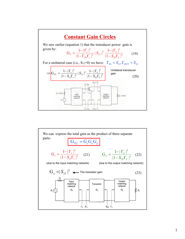
Constant Gain Circles We saw earlier (equation 1) that the transducer power gain is given by: 1− | Γs |2 1− | ΓL |2 2 GT = | S | (19) 21 2 2 | 1 − ΓIN Γs | | 1 − S 22 ΓL | For a unilateral case (i.e., S12=0) we have: ΓIN = S11 , ΓOUT = S22 ⇒ G TU = 1− | Γs |2 1− | ΓL |2 2 | S | 21 | 1 − S11Γs |2 | 1 − S22 ΓL |2 Unilateral transducer gain (20) We can express the total gain as the product of three separate parts: G TU = Gs GoGL Gs = 1− | Γs |2 | 1 − S11Γs |2 (21) (due to the input matching network) G o =| S 21 |2 1− | ΓL |2 GL = | 1 − S 22 ΓL |2 (22) (due to the output matching network) The transistor gain (23) 1 In decibels G TU (dB ) = Gs (dB ) + Go (dB ) + GL (dB ) (24) To Maximize Gs and GL we must have : Γs = S11* and * ΓL = S 22 (25) * * Using equations (21) and (22) with Γs = S11 and ΓL = S 22 we get” 1− | Γs |2 Gs = ⇒ | 1 − S11Γs |2 G s ,max = 1 1− | S11 |2 (26) 1− | ΓL |2 ⇒ GL = | 1 − S22 ΓL |2 G L ,max = 1 1− | S 22 |2 (27) Hence, the maximum GTU that we can get becomes: G TU ,max = Gs ,max GoGL ,max = 1 1 | S 21 |2 2 1− | S11 | 1− | S 22 |2 (28) 2 Unconditionally Stable Case, Sii < 1 It is obvious that when Γs = 1 or ΓL = 1 then Gs and GL will have the value of zero. 1− | Γs |2 Gs = | 1 − S11Γs |2 |Γs |=1 ⇒0 1− | ΓL |2 GL = | 1 − S11ΓL |2 |ΓL |=1 ⇒0 For any arbitrary value of Γs or ΓL will force Gs and GL to be between the values of zero and Gs,max or GL,max. The values of Γs and ΓL that yield constant gain values for solutions for Gs and GL lie on a circle that can be plotted on the Smith Chart. The circles have their centers located on the vectors drawn from * * the center of the Smith cahert to the point S11 or S22 . (See appendix D) The distance from the center of the Smith chart to the center of the constant gain circle along the vector Sii* is given by: g i Sii* C gi = 1− | S ii |2 (1 − g i ) (29) And the radius of the constant circle is: 1 − g i (1− | Sii |2 ) rg i = 1− | Sii |2 (1 − g i ) Where g i = (30) Gi 1− | Γi |2 = G i (1- | Sii |2 ) = (1- | Sii |2 ) 2 G i ,max | 1 − S ii Γi | (31) For either Gs or GL . Here the subscript i indicates either s or L. ii=11 for S11 and ii=22 for S22 3 Example: The S-parameters of a BJT measured at VCE=10V, IC=30 mA, and f=1GHz are given by: S 11 = 0 . 73 ∠175 o S 12 = 0 S 21 = 4 . 45 ∠ 65 o S 22 = 0 . 21 ∠ − 80 o • Calculate the optimum terminations • Calculate Gs,max, GL,max, and GTU, max in dB • Draw several Gs constant-gain circles • Design the input matching network for Gs=2 dB (1) Optimum terminations: Source Γs = S 11* = 0 . 73 ∠ − 175 o ⇒ Z s = ( 0 . 152 − j 0 .047 ) 50 Ω = 7 . 6 − j 2 . 35 Ω Load * ΓL = S 22 = 0 . 21 ∠ 80 o ⇒ Z L = ( 0 . 97 + j 0 . 43 ) 50 Ω = 48 . 5 + j 21 . 5 Ω (2) Gain: 1 = 2.141 or 3.31 dB 1− | S11 |2 1 = = 1.046 or 0.195 dB 1− | S22 |2 G s ,max = G L ,max G o =| S21 |2 = 19.8 or 12.97 dB G TU ,max (dB ) = 3.31 + 12.97 + 0.195 = 16.47 dB 4 (3) Constant Gain Circles for Gs (4) Input matching network Since the output network does not provide any gain we will keep the optimum termination at ΓL = S 22* = 0 . 21 ∠ 80 o and deal with the input network only! Any point of Γs along the Gs=2 dB circle will provide the o same gain. A point A on the circle will yield Γs = 0 . 43 ∠166 and a z s = 0 . 42 + j 0 . 1 on the Smith chart that can now be used to complete the input matching network. 5 Thus, the total GTU (db) can be evaluated as: since and G s = 2.0 dB and G L,max = 0.195 dB G o = 12.97 dB ⇒ G TU = 2 + 12.97 + 0.195 = 15.16 dB Note: This value is less than GTU,max of 16.47. Also note that the G=0 db gain circle always passes by the center of the Smith chart. Potentially Unstable Case, Sii > 1 1 Sii At that value we get infinite gain as shown in equation (31) The critical parameter in this case is Γi ,c = 1− | Γi |2 g i = G i (1- | Sii | ) = (1- | Sii |2 ) 2 | 1 − S ii Γi | 2 (31) To prevent oscillations at the input and output ports Γi must be selected such Re( Z s ) >| Re( Z IN ) | and Re( Z L ) >| Re( Z OUT ) | 6 Example: Let the S-parameters of a GaAS FET at f=1GHz be: S11 = 2.27∠ − 120o S 21 = 4∠50o S12 = 0 S 22 = 0.6∠ − 80o 1. Calculate the input impedance and the optimum output terminations 2. Determine the unstable region and construct the constant gain circles for Gs=5dB and Gs=3dB 3. Design the input matching network for Gs=3dB with the greatest degree of stability 1- Input impedance Draw the point 1 / S11* = 0.44∠ − 120o on the Smith chart ⇒ Z IN = 50( −0.5 − j 0.46) = −25 − j 23Ω 7 * The optimum output termination is given by: ΓL = S 22 = 0.6∠80o ⇒ Z L = (0.56 + j1.03) = 28 + j51.5 Ω (2) The stable region is where Re( Z s ) >| Re( Z IN ) | which is inside the big circle shown on the smith chart To draw the constant gain circles we need to locate 1/S11 and find the centers and the radii for the GS=5db and GS=3db For Gs=5db we get g s = 3.16[1 − (2.27) 2 ] = −13.123 1 + 13.123[1 − ( 2.27) 2 ] rg s = = 0.217 1 − (2.27) 2 (1 + 13.123) | C g s |= − 13.123(2.27) = 0.415 1 − (2.27) 2 (1 + 13.123) 8 (3) To obtain the greatest degree of stability we select the point A on the Gs=3 db circle such that it has the largest possible real part. Z s = 50(0.97 + j 0.5) = 48.5 + j 25Ω ⇒ Γs = 0.245∠79o or Unilateral Figure of Merit The design becomes simpler if the transistor device is unilateral (S12=0). In many practical cases S12 is small enough that it can be ignored. The maximum error caused by the this assumption is given by the ratio G T G TU This ratio is bounded by: where U= 1 G 1 < T < 2 (1 + U ) G TU (1 − U ) 2 | S12 || S 21 || S11 || S 22 | (1− | S11 |2 )(1− | S 22 |2 ) (32) Unilateral Figure of Merit (33) 9 For example look at the figure below. The max U occurs at 100 MHz and 1 GHz (U= -15db or U=0.03). Hence, we can write 1 G 1 < T < 2 (1 + 0.03) G TU (1 − 0.03) 2 − 0.26dB < or GT < 0.26dB G TU Max error=0.26 dB * For a conjugately matched unilateral device ( Γs = S11* and S22 ) then GTU becomes: GTU = 1 1 − S11 2 S21 2 1 1 − S22 (34) 2 Simultaneous Conjugate Match Bilateral case Only possible for K>1 * ΓL = ΓOUT ΓL* = S22 + S12 S21Γs 1 − S11Γs (35) * Γs = ΓIN Γs* = S11 + S12 S21ΓL 1 − S22 ΓL (36) 10 Using equations (35) and (36) lead to the values of Γs and ΓL that will yield simultaneously conjugate matching. ΓMs B1 ± B12 − 4 | C1 |2 = 2C1 ΓML = B2 ± B22 − 4 | C2 |2 2C1 (37) (38) B1 = 1+ | S11 |2 − | S 22 |2 − | ∆ |2 (39) B2 = 1+ | S22 |2 − | S11 |2 − | ∆ |2 (40) 11 * C1 = S11 − ∆S 22 (41) C2 = S 22 − ∆S11* (42) The maximum transducer under conjugate matching is given by: G T ,max or 1 1− | ΓML |2 2 = | S 21 | 1− | ΓMs |2 | 1 − S 22 ΓML |2 (43) G T ,max = | S 21 | ( K − K 2 − 1) | S12 | (44) G T ,min = | S 21 | ( K + K 2 − 1) | S12 | (45) Example: Design a microwave amplifier using a GaAs FET to operate at f=6 GHz with maximum transducer gain. S11 = 0 .641∠ − 171 .3o S12 = 0 .057 ∠16 .3o S 21 = 2 .058 ∠ 28 .5 o S 22 = 0 .572 ∠ − 95 .7 o Solution: K=1.504 and ∆ = 0.3014∠109.88o ⇒ unconditionally stable 12 S12 cannot be neglected. U=0.1085 and − 0.89 dB < To figure out ΓMs and GT < 1 dB G TU ΓML we need to calculate : B1 = 0.9928 B2 = 0.8255 C1 = 0.4786∠ − 177.3o C2 = 0.3911∠ − 103.9o ⇒ ΓMs = 0.762∠177.3o G T ,max = ΓML = 0.718∠103.9o | S21 | ( K − K 2 − 1) = 13.74 | S12 | Input Matching Network 7.2 − j1.23 YMs = = (144 − j 24.6) × 10 −3 S 50 13 Output Matching Network YML = 0.414 − j1.19 = (8.28 − j 23.8) ×10 −3 S 50 Amplifier network 14
