solutions
advertisement
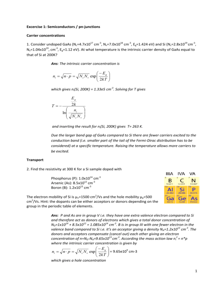
Excercise 1: Semiconductors / pn-junctions Carrier concentrations 1. Consider undoped GaAs (Nc=4.7x1017 cm-3, Nv=7.0x1018 cm-3, Eg=1.424 eV) and Si (Nc=2.8x1019 cm-3, Nv=1.04x10¹⁹, cm-3, Eg=1.12 eV). At what temperature is the intrinsic carrier density of GaAs equal to that of Si at 200K? Ans: The intrinsic carrier concentration is Eg ni n p N c N v exp 2kT which gives ni(Si, 200K) = 1.33e5 cm-3. Solving for T gives Eg T 2k ni ln N N c v and inserting the result for ni(Si, 200K) gives T= 263 K. Due the larger band gap of GaAs compared to Si there are fewer carriers excited to the conduction band (i.e. smaller part of the tail of the Fermi-Dirac distribution has to be considered) at a specific temperature. Raising the temperature allows more carriers to be excited. Transport 2. Find the resistivity at 300 K for a Si sample doped with Phosphorus (P): 1.0x1014 cm-3 Arsenic (As): 8.5x1012 cm-3 Boron (B): 1.2x1013 cm-3 The electron mobility of Si is µn=1500 cm2/Vs and the hole mobility µp=500 cm2/Vs. Hint: the dopants can be either acceptors or donors depending on the group in the periodic table of elements. Ans: P and As are in group V i.e. they have one extra valence electron compared to Si and therefore act as donors of electrons which gives a total donor concentration of ND=1x10¹⁴ + 8.5x1012 = 1.085x1014 cm-3. B is in group III with one fewer electron in the valence band compared to Si i.e. it’s an acceptor giving a density NA=1.2x1013 cm-3. The donors and acceptors compensate (cancel out) each other giving an electron concentration of n=ND-NA=9.65x1013 cm-3. According the mass action law ni2 = n*p where the intrinsic carrier concentration is given by Eg ni n p N c N v exp 2kT which gives a hole concentration = 9.65e109 cm-3 1 ni2 (9.65 109 ) 2 p 9.65 105 cm 3 13 n 9.65 10 Both electrons and hole contribute to the conductivity q(µn n µ p p) 1.6022 1019 (1500 9.65 1013 500 9.65 105 ) 0.0232 ( cm) 1 Giving a resistivity of 1 43.1 cm As can be seen, the hole concentration is so small (and the mobility is lower as well) so it can safely be ignored and the resistivity is set by the electron transport. 3. Calculate the electron and hole drift velocities through a 10-µm thick layer of intrinsic silicon across which a voltage of 1V is applied. Let µn = 1350 cm2/Vs and µp = 480 cm2/Vs. Ans: The electric field across the layer is ε=V / L = 1 (V) / 10-5 (m) = 105 V/m. The electron velocity is given by vn= ε∙µn = 105 (V/m) ∙ 1350∙10-4 (m2/Vs) = 13500 m/s The hole velocity is given by vp= ε∙µp = 105 (V/m) ∙ 480∙10-4 (m2/Vs) = 4800 m/s Note that the electric field is lower than the critical field for the onset of velocity saturation (see lecture 1). If the voltage would be increased >100V the carrier velocity would saturate and become independent of bias. 4. Holes (minority carriers) are steadily injected into a piece of n-doped Si (ND=1016 cm-3) at x=0 and extracted at x=W resulting in the hole concentration shown in the image below, where pn0 is the hole carrier concentration without injection. Use an intrinsic carrier concentration of ni=1.5*1010 cm-3 and W=5 µm. The hole mobility is µp = 480 cm2/Vs. Calculate the current density that flows in the xdirection. 2 Ans: The electron concentration is determined by the doping i.e. n≈ND. The equilibrium (without injection) hole (minority carriers) concentration is then given by the mass action law: pno= ni2/ND = (1.5 ∙1010)2 / 1016 = 22500 cm-3. The current density (due to diffusion of holes from 0 to W) is determined by the concentration gradient as kT dp( x) p 1000 pn 0 dp( x) q µ p kTµp n 0 dx 0 W q dx 1.38 10 23 J / K 300 K 480 cm 2 / Vs (1 1000) 22500 cm 3 8.93 10 8 A / cm 2 4 0 5 10 cm J p qD p The situation in the problem resembles that of the n-side of a forward biased pnjunction where minority carriers are steadily injected at the depletion region edge (x=0) and extracted at the contact (x=W). Since the minority carrier concentration decreases linearly there is no recombination in the region and the current is constant at each point. 3 pn-junctions / diodes 5a (problem 1.1 in book). Calculate the built-in potential, depletion layer depths and maximum field in an abrupt (not graded doping) pn junction in Si with doping densities NA=8*1015 cm-3 and ND=1017 cm-3 for three biases: - reverse bias of 5 V - zero bias - forward bias of 0.3 V 4 5b (problem 1.2 in book). Calculate the junction capacitance at a bias of 0, -3 and 0.5V. Assume a junction area of 2*10-5 cm2 5 6. For the circuits shown below using ideal diodes, find the values of the voltages and currents indicated. a) b) c) d) Ans The diode is forward biased i.e. its resistance is negligible and it can be treated as a short between the middle and lower terminals i.e. V = -5 V. The current is I=U/R= 5-(-5) [V] / 10 [kOhm] = 1 mA The diode is reverse biases i.e. its resistance is very high and it can be treated as an open circuit between the middle and lower terminals i.e. V = +5 V. The current I = 0 A. Diode is forward biased. V=5 V and I = 1 mA. Diode is reverse biased V=-5 V and I = 0 A. 7. a) At what forward voltage does a diode for which n=2 conduct a current equal to 1000Is (Is= saturation current at reverse bias)? b) Expressed in terms of Is, what current flows in the same diode when its forward voltage is 0.7V? Ans: a) Use the ideal diode equation I I S (e qV / nkT 1) Set I=1000IS and solve for V to get 1000 I S 2kT V ln 1 0.355 V IS q b) The ideal diode equation gives I I S (e qV / nkT 1) (e q 0.7 / nkT 1) 749 103 I s 6 8. A diode for which the forward voltage drop is 0.7 V at 1.0 mA and for which n=1 is operated at 0.5V. What is the value of the current? Ans: Use the ideal diode equation I I S (e qV / nkT 1) and solve for IS to get IS I (e qV / nkT 1) 10 3 1.602210190.7 / 1.3810 23300 (e 1) 1.78 10 12 mA Inserted in the diode equation this gives 19 I I S (e qV / nkT 1) 1.78 10 15 (e1.602210 0.5 / 1.381023300 1) 4.40 104 mA Note the very large difference in current of four orders of magnitude in the forward direction for only a change of 0.2 V. Equivalent circuits 9. Find the Thevenin and Norton equivalent circuits for the circuit shown below. Take care that you orient the polarity of the voltage source and the direction of the current source correctly relative to the terminals a and b. 7 8
