09 Heterojunction FET (HFET) principles
advertisement

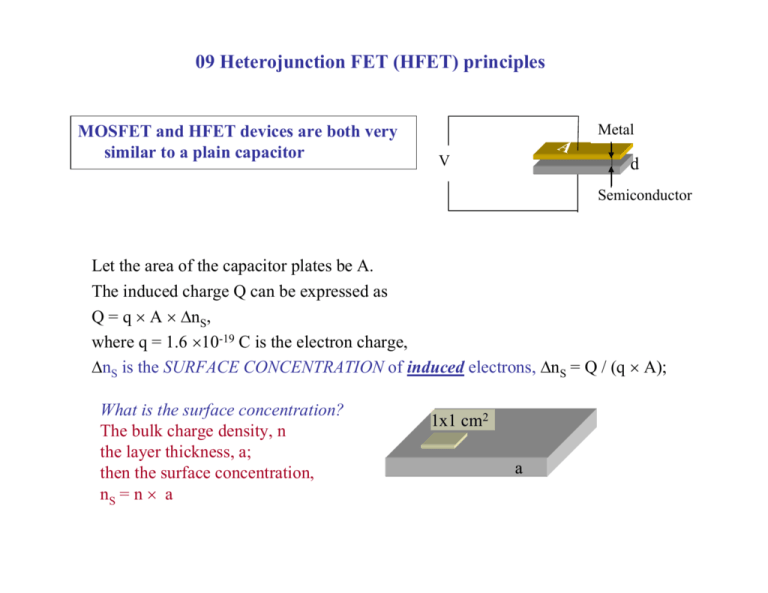
09 Heterojunction FET (HFET) principles MOSFET and HFET devices are both very similar to a plain capacitor Metal A V d Semiconductor Let the area of the capacitor plates be A. The induced charge Q can be expressed as Q = q × A × ∆nS, where q = 1.6 ×10⁻¹⁹ C is the electron charge, ∆nS is the SURFACE CONCENTRATION of induced electrons, ∆nS = Q / (q × A); What is the surface concentration? The bulk charge density, n the layer thickness, a; then the surface concentration, nS = n × a 1x1 cm2 a Estimation of induced charge Metal V A d Semiconductor For the PLAIN CAPACITOR, C = ε ε0 ×A/d Q = C × V = ε ε0 ×A×V/d, The induced concentration of electrons (which are negatively charged) in the top (metal) plate: ∆nSM = - ε ε0 ×V/(q×d) <0; in the bottom (semiconductor) plate: ∆nS = ε ε0 ×V/(q×d) >0; For a given voltage, V, the induced charge increases as we decrease d The threshold voltage of FETs Suppose the semiconductor plate is doped with donor concentration ND; The equilibrium electron concentration in the semiconductor, n0 = ND; For the layer thickness, a, the surface concentration nS0 = ND ×a; The voltage needed to deplete the entire active layer ( the semiconductor plate) is referred to as the THRESHOLD VOLTAGE of the FET For the n-doped layer the threshold voltage is negative in order to repulse the electrons. The induced concentration at the threshold has to compensate the equilibrium one: ∆nST = ε ε0 ×VT/(q×d) = - nS0 Therefore, VT = - q×d ×nS0/ (ε ε0) The charge control model of FETs At the threshold the net concentration in the channel is zero: ∆nST – nS0 = 0, where ∆nST = ε ε0 ×VT/(q×d) When the applied voltage is above the threshold, V > VT, ∆nS = ε ε0 ×V/(q×d) nS = ∆nS – ∆nST = ε ε0 /(q×d) × (V – VT) Note, ε ε0 /d = C1 the gap capacitance per unit area Therefore, nS = (C1/q) × (V – VT) The above model is referred to as “charge control model” of FETs FETs: general design considerations Low drain bias The gate length L The current through the channel is V0 I= R + where V0 is the voltage applied between the DRAIN and the SOURCE V- + V0 G S D Semiconductor We are assuming that V0 << VT (we will see why, later on) The channel resistance, R (Z is the device width): R= L qnµ aZ = L q ns µ Z The channel current is then: I = V0 (q nS µ Z) /L = V0 q µ Z (C1/q) × (V – VT) /L I = V0 µ Z C1 × (V – VT) /L FETs: general design considerations Low drain bias The gate length L I = V0 µ Z C1 × (V – VT) /L The transconductance, gm = dI/dV; The gm is the “responsivity” of FET. In the linear mode under consideration (V0 << V), gm = V0 µ Z C1 /L + - V- + V0 G S D Semiconductor The main factors affecting FET performance (for any FET type): µ I and gm L I and gm Carrier mobility in the channel and the gate length are crucial parameters of any FET Different types of FETs Metal - Oxide - Semiconductor FET (MOSFET) d W The gate-channel insulator is made out of dielectric (SiO2), ε = 3.9 Different types of FETs Junction FET (JFET) a0 W a The gate-channel insulator consists of the DEPLETION REGION, i.e. the same material as the channel. For GaAs, ε ~ 12; for GaN ε ~ 9. Different types of FETs Metal-Semiconductor FET (MESFET) a0 a The gate is formed by Schottky barrier to the semiconductor layer. The gate-channel insulator consists of the DEPLETION REGION, i.e. the same material as the channel. Very similar to the JFET The Heterojunction Field-Effect Transistor (HFET) The channel of HFETs is formed by 2D electron gas (2DEG) Channel induced channel (2DEG) electrons HFET JFET, MOSFET, MESFET Effects of high drain bias on FET characteristics MOSFET JFET + VG Source Gate + VD The gate- to drain voltage difference depends on the position along the gate So does the induced charge Drain Effects of high drain bias on FET characteristics The particular range of the gate voltage depends on the device type The channel narrowing at the drain edge of the gate causes current saturation in the FETs Effects of high drain bias on FET characteristics Electron velocity saturation due to high electric field in the channel Velocity saturation due to high electric field in the channel also results in the I-V saturation The average electric field in the channel, Eav ~ V0 /L Can be extremely high for small L I = V0 µ Z C1 × (V – VT) /L I = vS Z C1 × (V – VT) v = µ × E ~ µ × V0 /L The Heterojunction Field-Effect Transistor (HFET) The channel of HFETs is formed by 2D electron gas (2DEG) electrons induced channel (2DEG) after T.A. Fjeldly, T. Ytterdal and M. Shur, 1998 Undoped active layer Very high NS; very high µ; very high vS (in sub-µ HFETs) 1960 - Accumulation layer prediction (Anderson) 1969 - Enhanced mobility of 2DEG prediction (Esaki & Tsu) 1978 Enhanced mobility observed (Dingle et. al.) 1980 The first Heterojunction FET (HFET) 1991 The first GaN based HFET (A. Khan) The Heterojunction Field-Effect Transistor (HFET) A.k.a. High electron mobility FETs: why? 1) Mobility depends on the interactions between electrons and phonons and impurities. For the phonon scattering, the dependence of mobility on temperature: For the impurity scattering, the dependence of mobility on impurity concentration, N: When the dependence on both temperature and impurities is taken into account, The Heterojunction Field-Effect Transistor (HFET) Concentration dependence of electron mobility T = 300 K The Heterojunction Field-Effect Transistor (HFET) Electron Drift velocity The electron accelerates in the electric field until it gains enough energy to excite lattice vibrations: m n v n2 max = E n − E o ≈ hω l 2 where vnmax is the maximum electron drift velocity. Then the scattering process occurs, and the electron loses all the excess energy and all the drift velocity. Hence, the electron drift velocity varies between zero and vnmax, and average electron drift velocity (vn = vnmax/2) becomes nearly independent of the electric field: vn ≈ hω l = v sn 2m n Typically, vsn ≈ 105 m/s. Indeed, the measured drift velocity becomes nearly constant in high electric fields The Heterojunction Field-Effect Transistor (HFET) Electron Drift velocity 3 InGaAs electron velocity (100,000 m/s) InP GaAs 2 1 Heavily doped Si T = 300 K 0 0 5 10 15 20 electric field (kV/cm) In the heavily doped materials the peak electron velocity is lower The HFET basics metal AlGaAs GaAs qVN ∆E c qφb Ec Ec qVFB qϕb E Fi E Fp di Ev Considering first the band diagram of an AlGaAs/GaAs HFET with flat bands in the GaAs buffer. As can be seen from this figure, the flat-band voltage is given by VFB = φ b − V N − (∆Ec + ∆E F ) / q The HFET basics The HFET basics qVN F Fi Charge and field profiles Band diagram From the Poisson equation, Fi = qns ε 0ε s At the threshold, ns~0 --> Fi ~0 The HFET basics HFET threshold voltage When ns is close to zero, the Fermi level in the GaAs is close to the bottom of the conductance band. Therefore, qN d di2 − ∆Ec / q VT ≈ φ b − 2ε i For non-uniform doping profile, di N d (x) x dx VN = q ∫ ε (x) 0 i For the “delta-doped” barrier layer, VT ≈ φ b − qnδ dδ / ε i − ∆Ec / q The HFET basics HFET I-V characteristics Above the threshold the HFET is similar to MOSFET, i.e. qns = ci [VGT − V ( x )] where VGT = VG - VT The drain current: Id = Wµ n qns F = Wµ nc i (VGT − V ) [ ] dV dx ⎧ V V − V 2 / 2 , for V ≤ V DS SAT Wµ n ci ⎪ GT DS DS Id = ×⎨ L 2 ⎪⎩VGT / 2, for VDS > VSAT where VSAT = VGT The HFET basics HFET I-V characteristics The transconductance, gm = ⎧⎪βV , DS gm = ⎨ ⎪⎩βVGT , dId dVGS V DS for VDS ≤ VSAT for V DS >V SAT where β = Wµnci /L is called the transconductance parameter. The HFET basics HFET I-V characteristics Velocity saturation in HFETs A two-piece model is a simple, first approximation to a realistic velocity-field relationship: ⎧ µF , F < Fs v ( F) = ⎨ ⎩ vs , F ≥ Fs 1.2 m= More realistic velocity-field relationships : v ( F) = m=2 0.8 µF [1+ (µF / vs ) ] m=1 m 1/m where m = 1….2 0.4 0.0 0 1 2 Normalized Field 3 The HFET basics HFET I-V characteristics Velocity saturation in HFETs [ ] ⎧ V V −V2 / 2 , GT DS DS Wµ n ci ⎪ ×⎨ Id = L ⎪VL2 ⎡ 1 + (VGT V L )2 − 1⎤ , ⎥⎦ ⎩ ⎢⎣ for VDS ≤ VSAT for VDS > VSAT ⎡ ⎤ 2 VSAT = VGT − VL ⎢ 1+ (VGT / V L ) − 1⎥ ⎣ ⎦ where VL = Fs L. For VL >> VGT, we arrive to the same expression as with the constant mobility case. The HFET basics HFET I-V characteristics Velocity saturation in HFETs [ ] ⎧ V V −V2 / 2 , GT DS DS Wµ n ci ⎪ ×⎨ Id = L ⎪VL2 ⎡ 1 + (VGT V L )2 − 1⎤ , ⎥⎦ ⎩ ⎢⎣ for VDS ≤ VSAT for VDS > VSAT ⎡ ⎤ 2 VSAT = VGT − VL ⎢ 1+ (VGT / V L ) − 1⎥ ⎣ ⎦ where VL = Fs L. In the opposite limit, when VL << VGT, we obtain VSAT ≈ VL Isat ≈ βVLVGT where β = Wµnci /L is the transconductance parameter.


