mosfet - Electrical and Computer Engineering
advertisement
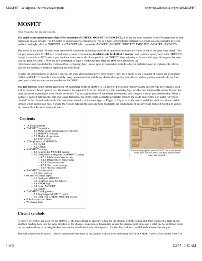
MOSFET - Wikipedia, the free encyclopedia http://en.wikipedia.org/wiki/MOSFET MOSFET From Wikipedia, the free encyclopedia The metal-oxide-semiconductor field-effect transistor (MOSFET, MOS-FET, or MOS FET), is by far the most common field-effect transistor in both digital and analog circuits. The MOSFET is composed of a channel of n-type or p-type semiconductor material (see article on semiconductor devices), and is accordingly called an NMOSFET or a PMOSFET (also commonly nMOSFET, pMOSFET, NMOS FET, PMOS FET, nMOS FET, pMOS FET). The 'metal' in the name (for transistors upto the 65 nanometer technology node) is an anachronism from early chips in which the gates were metal; They use polysilicon gates. IGFET is a related, more general term meaning insulated-gate field-effect transistor, and is almost synonymous with "MOSFET", though it can refer to FETs with a gate insulator that is not oxide. Some prefer to use "IGFET" when referring to devices with polysilicon gates, but most still call them MOSFETs. With the new generation of high-k technology that Intel and IBM have announced [1] (http://www.intel.com/technology/silicon/45nm_technology.htm) , metal gates in conjunction with the a high-k dielectric material replacing the silicon dioxide are making a comeback replacing the polysilicon. Usually the semiconductor of choice is silicon, but some chip manufacturers, most notably IBM, have begun to use a mixture of silicon and germanium (SiGe) in MOSFET channels. Unfortunately, many semiconductors with better electrical properties than silicon, such as gallium arsenide, do not form good gate oxides and thus are not suitable for MOSFETs. The gate terminal in the current generation (65 nanometer node) of MOSFETs is a layer of polysilicon (polycrystalline silicon; why polysilicon is used will be explained below) placed over the channel, but separated from the channel by a thin insulating layer of what was traditionally silicon dioxide, but more advanced technologies used silicon oxynitride. The next generation (45 nanometer and beyond) uses a high-k + metal gate combination. When a voltage is applied between the gate and source terminals, the electric field generated penetrates through the oxide and creates a so-called "inversion channel" in the channel underneath. The inversion channel is of the same type — P-type or N-type — as the source and drain, so it provides a conduit through which current can pass. Varying the voltage between the gate and body modulates the conductivity of this layer and makes it possible to control the current flow between drain and source. Contents 1 Circuit symbols 2 MOSFET operation 2.1 Metal-oxide-semiconductor structure 2.2 MOSFET structure 2.3 Modes of operation 2.4 Body effect 3 The primacy of MOSFETs 3.1 Digital 3.2 Analog 4 MOSFET scaling 4.1 Reasons for MOSFET scaling 4.2 Difficulties arising due to MOSFET scaling 4.2.1 Subthreshold conduction 4.2.2 Interconnect capacitance 4.2.3 Heat production 4.2.4 Gate oxide leakage 4.2.5 Process variations 5 MOSFET construction 5.1 Gate material 6 Other MOSFET types 6.1 Dual gate MOSFET 6.2 Depletion mode MOSFETs 6.3 NMOS logic 6.4 Power MOSFET 6.5 DMOS 7 MOSFET analog switch 7.1 Single-type MOSFET switch 7.2 Dual-type (CMOS) MOSFET switch 8 References and Notes 9 External links Photomicrograph of two MOSFETs in a test pattern. Probe pads for two gates and three source/drain nodes are labeled. Circuit symbols A variety of symbols are used for the MOSFET. The basic design is generally a line for the channel with the source and drain leaving it at right angles and then bending back into the same direction as the channel. Sometimes a broken line is used for enhancement mode and a solid one for depletion mode, but the awkwardness of drawing broken lines means this distinction is often ignored. Another line is drawn parallel to the channel for the gate. The bulk connection, if shown, is shown connected to the back of the channel with an arrow indicating PMOS or NMOS. Arrows always point from P to 1 of 8 2/2/07 10:42 AM MOSFET - Wikipedia, the free encyclopedia http://en.wikipedia.org/wiki/MOSFET N, so an NMOS (N-channel in P-well or P-substrate) has the arrow pointing in. If the bulk is connected to the source (as is generally the case with discrete devices) it is angled to meet up with the source leaving the transistor. If the bulk is not shown (as is often the case in IC design as they are generally common bulk) an inversion symbol is sometimes used to indicate PMOS. Comparison of enhancement and depletion mode symbols, along with JFET symbols: P-channel N-channel JFET MOSFET enh MOSFET dep For the symbols in which the bulk, or body, terminal is shown, it is here shown internally connected to the source. This is a typical configuration, but by no means the only important configuration. In general, the MOSFET is a four-terminal device, and in integrated circuits many of the MOSFETs share a body connection, not necessarily connected to the source terminals of all the transistors. MOSFET operation Metal-oxide-semiconductor structure A traditional metal-oxide-semiconductor (MOS) structure is obtained by depositing a layer of silicon dioxide (SiO2 ) and a layer of metal (polycrystalline silicon is actually used instead of metal) on top of a semiconductor die. As the silicon dioxide is a dielectric material its structure is equivalent to a plane capacitor, with one of the electrodes replaced by a semiconductor. When a voltage is applied across a MOS structure, it modifies the distribution of charges in the semiconductor. If we consider a P-type semiconductor (with NA the density of holes), a positive VGB (see figure) tends to reduce the concentration of holes and increase the concentration of electrons. If VGB is high enough, the concentration of negative charge carriers near the gate is more than that of positive charges, in what is known as an inversion layer. Metal-oxide-semiconductor structure This structure with P-type body is the basis of the N-type MOSFET, which requires the addition of an N-type source and drain regions. MOSFET structure A metal-oxide-semiconductor field-effect transistor (MOSFET) is based on the modulation of charge concentration caused by a MOS capacitance. It includes two terminals (source and drain) each connected to separate highly doped regions. These regions can be either P or N type, but they must both be of the same type. The highly doped regions are typically denoted by a '+' following the type of doping (see the image at the right). These two regions are separated by a doped region of opposite type, known as the body. This region is not highly doped, denoted by the lack of a '+' sign. The active region constitutes a MOS capacitance with a third electrode, the gate, which is located above the body and insulated from all of the other regions by an oxide. Cross Section of an NMOS If the MOSFET is an N-Channel or nMOS FET, then the source and drain are 'N+' regions and the body is a 'P' region. When a positive gate-source voltage is applied, it creates an N-channel at the surface of the P region, just under the oxide, by depleting this region of holes. This channel extends between the source and the drain, but current is conducted through it only when the gate potential is high enough to attract electrons from the source into the channel. When zero or negative voltage is applied between gate and source, the channel disappears and no current can flow between the source and the drain. If the MOSFET is an P-Channel or pMOS FET, then the source and drain are 'P+' regions and the body is a 'N' region. When a negative gate-source voltage (positive source-gate) is applied, it creates a P-channel at the surface of the N region, just under the oxide, by depleting this region of electrons. This channel extends between the source and the drain, but current is conducted only when the gate potential is low enough to attract holes from the source into the channel. When a near-zero or positive voltage is applied between gate and body, the channel disappears and no current can flow between the source and the drain. The source is so named because it is the source of the charge carriers (electrons for N-channel, holes for P-channel) that flow through the channel; similarly, the drain is where the charge carriers leave the channel. 2 of 8 2/2/07 10:42 AM MOSFET - Wikipedia, the free encyclopedia http://en.wikipedia.org/wiki/MOSFET Modes of operation The operation of a MOSFET can be separated into three different modes, depending on the voltages at the terminals. For an enhancement mode, n-channel MOSFET the modes are: Cut-off or sub-threshold mode When VGS < Vth where V th is the threshold voltage of the device. According to the threshold model, the transistor is turned off, and there is no conduction between drain and source. In reality, the Boltzmann distribution of electron energies allows some of the more energetic electrons at the source to enter the channel and flow to the drain, resulting in a subthreshold current that is an exponential function of gate–source voltage. While the current between drain and source should ideally be zero when the transistor is being used as a turned-off switch, there is a weak-inversion current, sometimes called subthreshold leakage. Triode or linear region When VGS > Vth and VDS < VGS - Vth The transistor is turned on, and a channel has been created which allows current to flow between the drain and source. The MOSFET operates like a resistor, controlled by the gate voltage relative to both the source and drain voltages. The current from drain to source is modeled as: Evolution of the drain current of a MOSFET with the drain-to-source voltage for several VGS - Vth values. where μ n is the charge-carrier mobility, W is the gate width, L is the gate length and Cox is the gate oxide capacitance per unit area. The transition from the exponential subthreshold region to the triode region is not as sharp as the equations suggest. Cross section of a MOSFET operating in the linear region Saturation When VGS > Vth and VDS > VGS - Vth The switch is turned on, and a channel has been created, which allows current to flow between the drain and source. Since the drain voltage is higher than the gate voltage, a portion of the channel is turned off. The onset of this region is also known as pinch-off. The drain current is now relatively independent of the drain voltage (in a first-order approximation) and the current is controlled by only the gate–source voltage, modeled as: this equation can be multiplied by (1 + λVDS) to take into account the channel length modulation (Early effect). Cross section of a MOSFET operating in the saturation region Body effect The body effect describes the changes in the threshold voltage by the change in the source-bulk voltage, approximated by the following equation: , where V TO is the zero substrate bias, γ is the body effect parameter, and 2φ is the surface potential parameter. The body can be operated as a second gate, and is sometimes referred to as the "back gate"; the body effect is sometimes called the "back-gate effect". (http://equars.com/~marco/poli/phd/node20.html) The primacy of MOSFETs In 1960, Dawon Kahng and Martin Atalla at Bell Labs invented the metal oxide semiconductor field-effect transistor (MOSFET). Theoretically different from Shockley's transistor, the MOSFET was structured by putting an insulating layer on the surface of the semiconductor and then placing a metallic gate electrode on that. It used crystalline silicon for the semiconductor and a thermally oxidized layer of silicon dioxide for the insulator. Not only did it possess such technical attractions as low cost of production and ease of integration, the silicon MOSFET did not generate localized electron traps (interface states) at the interface between the silicon and its native oxide layer, and thus was free of the characteristic that had impeded the performance of earlier transistors. Buoyed by this stroke of good fortune, the MOSFET has achieved electronic hegemony. It is this serendipity that sustains the large-scale integrated circuits (LSIs) underlying today's information society. The MOSFET has become the basic element of all silicon integrated circuits. The basic device was conceived by Lilienfeld in the 1920’s,[1] but he had no platform on which to build the device. The silicon planar process conceived in the late 1950’s by McCaldin and Hoerni[2] and the integrated circuit conceived by Kilby and Noyce[3] was that platform that was needed to allow Lilienfeld’s device to be realized in the modern era. Atalla and Khang[4] then described the modern MOSFET in the late 1950’s and Hofstein and Heiman in 1963[5] described the structure of the MOSFET on the silicon planar process platform. However this planar MOSFET paled in comparison to the Bipolar Junction Transistor (BJT) conceived by Shockley, Bardeen, Brattain.[6] This early MOSFET was very difficult to use in integrated circuit design because of the uncertainty of the placement of the gate with respect to the source and drain, and slow because of the relative size of the gate. Bower[7] solved both of these problems by using the gate structure itself as the mask or template to define the placement of the source and drain with respect to the gate. This simple step eliminated the uncertainty of the placement of 3 of 8 2/2/07 10:42 AM MOSFET - Wikipedia, the free encyclopedia http://en.wikipedia.org/wiki/MOSFET the gate which solved the integrated circuit design problem and this also solved the speed problem which provided the theoretically smallest possible gate to be used in the formation of the device. Bower and Dill[8] described the Self-Aligned-Gate MOSFET or SAGFET made with either a metal or polysilicon gate. Faggin and Klein developed a working silicon-gate process at Fairchild in 1968.[9] The silicon-gate SAGFET surpassed the BJT in the 1970’s to become the device of choice used by all modern integrated circuits. The SAGFET has become the most replicated man-made inorganic structure in the history of mankind. Digital The growth of digital technologies like the microprocessor has provided the motivation to advance MOSFET technology faster than any other type of silicon-based transistor. The principal reason for the success of the MOSFET was the development of digital CMOS logic, which uses p- and n-channel MOSFETs as building blocks. The great advantage of CMOS logic is that they allow no current to flow (ideally), and thus no power to be consumed, except when the inputs to logic gates are being switched. CMOS accomplishes this by complementing every nMOSFET with a pMOSFET and connecting both gates and both drains together. A high voltage on the gates will cause the nMOSFET to conduct and the pMOSFET not to conduct and a low voltage on the gates causes the reverse. During the switching time the voltage goes from one state to another and both will conduct. This arrangement greatly reduces power consumption and heat generation. Overheating is a major concern in integrated circuits, since ever more transistors are packed into ever smaller chips. Another advantage of MOSFETs for digital switching is that the oxide layer between the gate and the channel prevents DC current from flowing through the gate, further reducing power consumption and giving a very large input impedance. The insulating oxide between the gate and channel effectively isolates a MOSFET in one logic stage from earlier and consequent stages, which allows to drive a considerable number of MOSFET inputs from a single MOSFET output. Bipolar transistor-based logics (such as TTL) do not have such a high fanout capacity. This isolation also makes it easier for the designers to ignore to some extent loading effects between logic stages independently. That extent is defined by the operating frequency: as frequencies increase, the input impedance of the MOSFETs decreases. Analog The MOSFET's strengths as the workhorse transistor in most digital circuits do not translate into supremacy in analog circuits. The bipolar junction transistor (BJT) has traditionally been the analog designer's transistor of choice, due largely to its high transconductance and unique properties. Nevertheless, MOSFETs are widely relied upon for analog purposes as well. Some of the advantages of MOSFETs are that due to their positive temperature coefficient, they do not suffer as much from thermal runaway as BJTs do and that their linear region allows them to be used as precision resistors, which can have a much higher controlled resistance than BJTs. Also, they can be formed into capacitors and specialized circuits allow op-amps made from them to appear as inductors, thereby allowing all of the normal analog devices, except for diodes (which can be made smaller than a MOSFET anyway), to be built entirely out of MOSFETs. This allows for complete analog circuits to be made on a silicon chip in a much smaller space. Some ICs combine analog and digital MOSFET circuitry on a single chip, making the needed board space even smaller. This creates a need to isolate the analog circuits from the digital circuits on a chip level, leading to the use of isolation rings and Silicon-On-Insulator (SOI). The main advantage of BJTs vs MOSFETs in the analog design process is the ability of BJTs to handle a larger current in a smaller space. Fabrication processes exist that incorporate BJTs and MOSFETs into a single device, these mixed-transistor devices are called Bi-FETs (Bipolar-FETs) if they contain just one BJT-FET and BiCMOS (bipolar-CMOS) if they contain complementary BJT-FETs. This device provides for the advantages of both the insulated gate and the higher current density. The BJT also has some advantages over the MOSFET in certain digital circuits. BJTs are currently better for at least 2 digital jobs. The first is in high speed switching because they don't have the "larger" capacitance from the gate, which when multiplied by the resistance of the channel gives the intrinsic time constant of the process. The intrinsic time constant places a limit on the speed a MOSFET can operate at because higher frequency signals are filtered out. Widening the channel reduces the resistance of the channel, but increases the capacitance by the exact same amount. Reducing the width of the channel increases the resistance, but reduces the capacitance by the same amount. R*C=Tc1, 0.5R*2C=Tc1, 2R*0.5C=Tc1. There is no way to minimize the intrinsic time constant for a certain process. Different processes using different channel lengths, channel heights, gate thicknesses and materials will have different intrinsic time constants. You can skip most of this problem with a BJT because it doesn't have a gate. The second job stems from the first. When driving many other gates, called fanning out, the resistance of the MOSFET is in series with the gate capacitances of the other FETs, creating a secondary time constant. Delay circuits use this fact to create a set signal delay by using a small CMOS device to send a signal to many other, many times larger CMOS devices. The secondary time constant can be minimized by increasing the driving FETs channel width to decrease its resistance and decreasing the channel width of the FETs being driven, decreasing their capacitance. This does have a drawback because it increases the capacitance of the driving FET and increases the resistance of the FETs being driven, but usually those drawbacks are a minimal problem when compared to the timing problem. BJTs are better to drive the other gates because they can output more current than MOSFETs, allowing for the FETs being driven to charge faster. Many chips will employ MOSFET inputs and BiCMOS (see above paragraph) outputs. MOSFET scaling Over the past decades, the MOSFET has continually been scaled down in size; typical MOSFET channel lengths were once several micrometres, but modern integrated circuits are incorporating MOSFETs with channel lengths of less than a tenth of a micrometre. Indeed Intel began production of a process featuring a 65 nm feature size (with the channel being even shorter) in early 2006. Until the late 1990s, this size reduction resulted in great improvement to MOSFET operation with no deleterious consequences. Historically, the difficulties with decreasing the size of the MOSFET have been associated with the semiconductor device fabrication process. 4 of 8 2/2/07 10:42 AM MOSFET - Wikipedia, the free encyclopedia http://en.wikipedia.org/wiki/MOSFET Reasons for MOSFET scaling Smaller MOSFETs are desirable for several reasons. First, smaller MOSFETs may allow more current to pass, due to their shorter length dimension; conceptually, MOSFETs are like resistors in the on-state, and shorter resistors have less resistance; however, they may also have smaller widths, leading to proportionally higher resistance, so the real issue is whether the ohms per square is reduced. Second, smaller MOSFETs have smaller gate areas, and thus lower gate capacitance. Scaled MOSFETs also have thinner gate dielectrics, which reduces the on-state ohms per square but makes the gate capacitance per unit area higher; nevertheless, these effects still both go in the right direction. These first two factors contribute to lower switching times, and thus higher processing speeds, and lower energy per switching event. A third reason for MOSFET scaling is reduced area, leading to reduced cost. Smaller MOSFETs can be packed more densely, resulting in either smaller chips or chips with more computing power in the same area. Since fabrication costs for a semiconductor wafer are relatively fixed, the cost per integrated circuits is mainly related to the number of chips that can be produced per wafer. Hence, smaller ICs allow more chips per wafer, reducing the price per chip. Difficulties arising due to MOSFET scaling Producing MOSFETs with channel lengths smaller than a micrometre is a challenge, and the difficulties of semiconductor device fabrication are always a limiting factor in advancing integrated circuit technology. Recently, the small size of the MOSFET has created operational problems. Subthreshold conduction Because of small MOSFET geometries, the voltage that can be applied to the gate must be reduced to maintain reliability. To maintain performance, the threshold voltage of the MOSFET has to be reduced as well. As threshold voltage is reduced, the transistor cannot be completely turned off; that is, the transistor operates in weak-inversion mode, with a subthreshold leakage, or subthreshold conduction, between source and drain. Subthreshold conduction, which was ignored in the past, now can consume upwards of half of the total power consumption of modern high-performance VLSI chips. Some micropower analog circuits are designed to take advantage of subthreshold conduction; by working in the weak-inversion region, the MOSFETs in these circuits deliver the highest possible transconductance-to-current ratio. Interconnect capacitance Traditionally switching time was roughly proportional to the gate capacitance of gates. However, with transistors becoming smaller and more transistors being placed on the chip, interconnect capacitance (the capacitance of the wires connecting different parts of the chip) is becoming a large percentage of capacitance. Signals have to travel through the interconnect, which leads to increased delay and lower performance. Heat production The ever-increasing density of MOSFETs on an integrated circuit is creating problems of substantial localized heat generation that can impair circuit operation. Circuits operate slower at high temperatures, and have reduced reliability and shorter lifetimes. Heat sinks and other cooling methods are now required for many integrated circuits including microprocessors. Power MOSFETs are at risk of thermal runaway. As their on-state resistance rises with temperature, the power loss on the junction rises correspondingly, generating further heat. When the heatsink is not able to keep the temperature low enough, the junction temperature may rise quickly and uncontrollably, resulting in destruction of the device. Gate oxide leakage The gate oxide, which serves as insulator between the gate and channel, should be made as thin as possible to increase the channel conductivity and performance when the transistor is on and to reduce subthreshold leakage when the transistor is off. However, with current gate oxides with a thickness of around 1.2 nm (which in silicon is ~5 atoms thick) the quantum mechanical phenomenon of electron tunneling occurs between the gate and channel, leading to increased power consumption. Insulators (referred to as high-k dielectrics) that have a larger dielectric constant than silicon dioxide, such as group IVb metal silicates e.g. hafnium and zirconium silicates and oxides are going to be used to reduce the gate leakage from the 45 nanometer technology node onwards. Increasing the dielectric constant of the gate oxide material allows a thicker layer while maintaining a high capacitance. The higher thickness reduces the tunneling current between the gate and the channel. An important consideration is the barrier height of the new gate oxide; the difference in conduction band energy between the semiconductor and the oxide (and the corresponding difference in valence band energy) will also affect the leakage current level. For the traditional gate oxide, silicon dioxide, the former barrier is approximately 8 eV. For many alternative dielectrics the value is significantly lower, somewhat negating the advantage of higher dielectric constant. Process variations With MOSFETS becoming smaller, the number of atoms in the silicon that produce many of the transistor's properties is becoming fewer. During chip manufacturing, random process variation can affect the size of the transistor, which becomes a greater percentage of the overall transistor size as the transistor shrinks. The transistor characteristics become less deterministic, but more statistical. This statistical variation increases design difficulty. 5 of 8 2/2/07 10:42 AM MOSFET - Wikipedia, the free encyclopedia http://en.wikipedia.org/wiki/MOSFET MOSFET construction Gate material The primary criterion for the gate material is that it is a good conductor. Highly-doped polycrystalline silicon is an acceptable, but certainly not ideal conductor, and it also suffers from some more technical deficiencies in its role as the standard gate material. Nevertheless, there are several reasons favoring use of polysilicon as a gate material: 1. The threshold voltage (and consequently the drain to source on-current) is modified by the work function difference between the gate material and channel material. Because polysilicon is a semiconductor, its work function can be modulated by adjusting the type and level of doping. Furthermore, because polysilicon has the same bandgap as the underlying silicon channel, it is quite straightforward to tune the work function, so as to achieve low threshold voltages for both NMOS and PMOS devices. By contrast the work functions of metals are not easily modulated, so tuning the work function to obtain low threshold voltages becomes a significant challenge. Additionally, obtaining low threshold devices on both PMOS and NMOS devices would likely require the use of different metals for each device type, adding additional complexity to the fabrication process. 2. The Silicon-SiO2 interface has been well studied and is known to have relatively few defects. By contrast many metal-insulator interfaces contain significant levels of defects which can lead to fermi-level pinning, charging, or other phenomena that ultimately degrade device performance. 3. In the MOSFET IC fabrication process, it is preferable to deposit the gate material prior to certain high-temperature steps in order to make better performing transistors. Such high temperature steps would melt some metals, limiting the types of metals that could be used in a metal-gate based process. While polysilicon gates have been the defacto standard for the last twenty years, they do have some disadvantages, which have led to the announcement of their replacement by metal gates. These disadvantages include: 1. Polysilicon is not a great conductor (approximately 1000 times more resistive than metals) which reduces the signal propagation speed through the material. The resistivity can be lowered by increasing the level of doping, but even highly doped polysilicon is not as conductive as most metals. In order to improve conductivity further, sometimes a high temperature metal such as tungsten, titanium, cobalt, and more recently nickel, is alloyed with the top layers of the polysilicon. Such a blended material is called silicide. The silicide-polysilicon combination has better electrical properties than polysilicon alone and still does not melt in subsequent processing. Also the threshold voltage is not significantly higher than polysilicon alone, because the silicide material is not near the channel. The process in which silicide is formed on both the gate electrode and the source and drain regions is sometimes called salicide, self-aligned silicide. 2. When the transistors are extremely scaled down, it is necessary to make the gate dielectric layer very thin, around 1 nm in state-of-the-art technologies. A phenomenon observed here is the so-called poly depletion, where a depletion layer is formed in the gate polysilicon layer next to the gate dielectric when the transistor is in the inversion. To avoid this problem a metal gate is desired. A variety of metal gates such as tantalum, tungsten, tantalum nitride, and titanium nitride, usually in conjunction with high-k dielectrics. An alternative is to use fully-silicided polysilicon gates, and the process is referred to as FUSI. Other MOSFET types Dual gate MOSFET The dual gate MOSFET has a tetrode configuration, where both gates control the current in the device. It is commonly used for small signal devices in radio frequency applications where the second gate is normally used for gain control or mixing and frequency conversion. Depletion mode MOSFETs There are depletion mode MOSFET devices, which are less commonly used than the standard enhancement mode devices already described. These are MOSFET devices which are doped so that a channel exists even without any voltage applied to the gate. In order to control the channel, a negative voltage is applied to the gate, depleting the channel which reduces the current flow through the device. In essence, the depletion mode device is equivalent to a normally closed switch, while the enhancement mode device is equivalent to a normally open switch.[2] (http://www.techweb.com/encyclopedia/imageFriendly.jhtml;jsessionid=VDNZQOUDRXA1OQSNDBCSKHSCJUMEKJVN?term=depletion+mode) NMOS logic n-channel MOSFETs are smaller than p-channel MOSFETs and producing only one type of MOSFET on a silicon substrate is cheaper and technically simpler. These were the driving principles in the design of NMOS logic which uses n-channel MOSFETs exclusively. However, unlike CMOS logic, NMOS logic consumes power even when no switching is taking place. With advances in technology, CMOS logic displaced NMOS logic in the 1980s to become the preferred process for digital chips. Power MOSFET 6 of 8 2/2/07 10:42 AM MOSFET - Wikipedia, the free encyclopedia http://en.wikipedia.org/wiki/MOSFET Power MOSFETs have a different structure than the one presented above.[10] As with all power devices, the structure is vertical and not planar. Using a vertical structure, it is possible for the transistor to sustain both high blocking voltage and high current. The voltage rating of the transistor is a function of the doping and thickness of the N epitaxial layer (see cross section), while the current rating is a function of the channel width (the wider the channel, the higher the current). In a planar structure, the current and breakdown voltage ratings are both function of the channel dimensions (respectively width and length of the channel), resulting in inefficient use of the "silicon estate". With the vertical structure, the component area is roughly proportional to the current it can sustain, and the component thickness (actually the N-epitaxial layer thickness) is proportional to the breakdown voltage. It is worth noting that power MOSFETs with lateral structure exist. They are mainly used in high-end audio amplifiers. Their advantage is a better behaviour in the saturated region (corresponding to the linear region of a bipolar transistor) than the vertical MOSFETs. Vertical MOSFETs are designed for switching applications, so they are only used in On or Off states. Cross section of a Power MOSFET, with square cells. A typical transistor is constituted of several thousand cells DMOS DMOS stands for double-Diffused Metal Oxide Semiconductor. Most of the power MOSFETs are made using this technology. MOSFET analog switch MOSFET analog switches use the MOSFET channel as a low–on-resistance switch to pass analog signals when on, and as a high impedance when off. Signals flow in both directions across a MOSFET switch. In this application the drain and source of a MOSFET exchange places depending on the voltages of each electrode compared to that of the gate. For a simple MOSFET without an integrated diode, the source is the more negative side for an N-MOS or the more positive side for a P-MOS. All of these switches are limited on what signals they can pass or stop by their gate-source, gate-drain and source-drain voltages, and source-to-drain currents; exceeding the voltage limits will potentially damage the switch. Single-type MOSFET switch This analog switch uses a four-terminal simple MOSFET of either P or N type. In the case of an N-type switch, the body is connected to the most negative supply (usually GND) and the gate is used as the switch control. Whenever the gate voltage exceeds the source voltage by at least a threshold voltage, the MOSFET conducts. The higher the voltage, the more the MOSFET can conduct. An N-MOS will pass through all voltages less than (Vgate-Vtn). When the switch is conducting, it typically operates in the saturation region, since the source and drain voltages will typically be nearly equal. In the case of a P-MOS, the body is connected to the most positive voltage, and the gate is brought to a lower potential to turn the switch on. The P-MOS switch passes all voltages higher than (Vgate+Vtp). A P-MOS switch will have about three times the resistance of an N-MOS device of equal dimensions because electrons have three times the mobility of holes in silicon. Dual-type (CMOS) MOSFET switch This "complementary" or CMOS type of switch uses one P-MOS and one N-MOS FET to counteract the limitations of the single-type switch. The FETs have their drains and sources connected in parallel, the body of the P-MOS is connected to the high potential (VDD) and the body of the N-MOS is connected to the low potential (Gnd). To turn the switch on the gate of the P-MOS is driven to the low potential and the gate of the N-MOS is driven to the high potential. For voltages between (VDD-Vtn) and (Gnd+Vtp) both FETs conduct the signal, for voltages less than (Gnd+Vtp) the N-MOS conducts alone and for voltages greater than (VDD-Vtn) the P-MOS conducts alone. The only limits for this switch are the gate-source, gate-drain and source-drain voltage limits for both FETs. Also, the P-MOS is typically three times the width of the N-MOS so the switch will be balanced. Tri-state circuitry sometimes incorporates a CMOS MOSFET switch on its output to provide for a low ohmic, full range output when on and a high ohmic, mid level signal when off. References and Notes 1. ^ Lilienfeld, J. E., U.S. Patent 1,900,018 filed March 28, 1928, issued March 7, 1933 2. ^ McCaldin, Hoerni, independently conceived the Planar Process. Hoerni presented a paper "Planar Silicon Transistors and Diodes," at the 1960 Electron Devices Meeting, Washington, D.C. 3. ^ Kilbey, Noyce, Conceived independently by both, Kilby received the Nobel Price Physics 2000 after Noyce’s death. 4. ^ Khang, D. and Atalla, M. M., IRE Solid State Device Res. Conf., Pittsburgh, 1960. 5. ^ Hofstein & Heiman, Proceedings of the IEEE, September 1963. 6. ^ William B. Shockley, John Bardeen, Walter H. Brattain, Nobel Prize in Physics 1956 7. ^ Bower, U.S. Patent 3,472,712, conceived July 1965, filed October 27, 1966, issued October 14, 1969. 8. ^ R. W. Bower and H. G. Dill, "Insulated-gate field-effect transistors fabricated using the gate as source–drain mask", Paper 16.6 International Electron Device Meeting, Washington, D.C., 1966. 9. ^ F. Faggin and T. Klein, "Silicon Gate Technology," Solid-State Electronics, vol. 13, Aug. 1970, pp. 1125-1144. 7 of 8 2/2/07 10:42 AM MOSFET - Wikipedia, the free encyclopedia http://en.wikipedia.org/wiki/MOSFET 10. ^ Power Semiconductor Devices, B. Jayant Baliga, PWS publishing Company, Boston. ISBN 0-534-94098-6 External links MOSFET applet (http://www-g.eng.cam.ac.uk/mmg/teaching/linearcircuits/mosfet.html) Very nice applet that helps to understand MOSFET. MOSFET models (http://web.cs.mun.ca/~paul/transistors/node3.html) Diagrams and mathematical derivation. MIT Open Courseware 6.002 (http://ocw.mit.edu/OcwWeb/Electrical-Engineering-and-Computer-Science/6-002Circuits-and-ElectronicsFall2000/VideoLectures/index.htm) -Link to the intro electrical engineering course at MIT on circuits and electronics. MIT Open Courseware 6.012 (http://ocw.mit.edu/OcwWeb/Electrical-Engineering-and-Computer-Science/6-012Fall-2005/LectureNotes/index.htm) -- Link to a more advanced class taught at MIT all about microelectronics and MOSFETs Retrieved from "http://en.wikipedia.org/wiki/MOSFET" Category: Transistors This page was last modified 23:03, 31 January 2007. All text is available under the terms of the GNU Free Documentation License. (See Copyrights for details.) Wikipedia® is a registered trademark of the Wikimedia Foundation, Inc., a US-registered 501(c)(3) tax-deductible nonprofit charity. 8 of 8 2/2/07 10:42 AM


