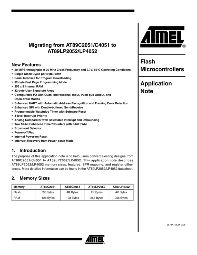
Migrating from AT89C2051/C4051 to
AT89LP2052/LP4052
New Features
•
•
•
•
•
•
•
•
•
•
•
•
•
•
•
•
•
20 MIPS throughput at 20 MHz Clock Frequency and 2.7V, 85°C Operating Conditions
Single Clock Cycle per Byte Fetch
Serial Interface for Program Downloading
32-byte Fast Page Programming Mode
256 x 8 Internal RAM
32-byte User Signature Array
Configurable I/O with Quasi-bidirectional, Input, Push-pull Output, and
Open-drain Modes
Enhanced UART with Automatic Address Recognition and Framing Error Detection
Enhanced SPI with Double-buffered Send/Receive
Programmable Watchdog Timer with Software Reset
4-level Interrupt Priority
Analog Comparator with Selectable Interrupt and Debouncing
Two 16-bit Enhanced Timer/Counters with 8-bit PWM
Brown-out Detector
Power-off Flag
Internal Power-on Reset
Interrupt Recovery from Power-down Mode
Flash
Microcontrollers
Application
Note
1. Introduction
The purpose of this application note is to help users convert existing designs from
AT89C2051/C4051 to AT89LP2052/LP4052. This application note describes
AT89LP2052/LP4052 memory sizes, features, SFR mapping, and register differences. More detailed information can be found in the AT89LP2052/LP4052 datasheet.
2. Memory Sizes
Memory
AT89C2051
AT89C4051
AT89LP2052
AT89LP4052
Flash
2K Bytes
4K Bytes
2K Bytes
4K Bytes
RAM
128 Bytes
128 Bytes
256 Bytes
256 Bytes
3573A–MCU–7/05
3. Single Clock Cycle per Byte Fetch
The AT89LP2052/LP4052 is built around an enhanced CPU core that can fetch a single byte
from memory every clock cycle.
4. Serial Interface for Program Downloading
The program memory can be programmed using the 4 SPI pins while RST is strapped to VCC.
Programming through the serial interface shares the same command format as programming
through the parallel interface.
5. 32-byte Fast Page Programming Mode
Up to 32 bytes of data can be loaded to be written at any time. The Load Code Page Buffer command allows for interrupted loading of 32 bytes of data that can be written later. The Write Code
Page command can write a previously loaded page of data or load and write anywhere from 1 to
32 bytes of data to code memory.
6. 32-byte User Signature Array
Thirty-two bytes are accessible to the user to program their own desired data. Bytes can be
either programmed by parallel or serial mode.
7. Configurable I/O with Quasi-bidirectional, Input, Push-pull Output, and
Open-drain Modes
All 15 port pins can be configured to one of four modes:
1. Quasi-bidirectional Output mode pins function similar to 8051 port pins.
2. Input-only Mode is a Schmitt-triggered input for improved noise rejection.
3. Open-drain Output configuration turns off all pull-ups and only drives the pull-down
translator of the port pin when the port register contains a logic “0”.
4. Push-pull Output configuration has the same pull-down structure as both the opendrain and quasi-bidirectional output modes, but provides a continuous strong pull-up
when the port register contains a logic “1”.
All port pins default to input-only mode after reset. Port modes may be assigned in software on a
pin-by-pin basis.
8. Enhanced UART with Automatic Address Recognition and Framing
Error Detection
When used for frame error detection, the UART looks for missing stop bits in the communication.
A missing bit will set the FE bit in the SCON Register. Automatic Address Recognition allows the
UART to recognize certain addresses in the serial bit stream by using hardware to make the
comparison.
9. Enhanced SPI with Double-buffered Send/Receive
The enhanced SPI mode allows the write buffer to hold the next byte to be transmitted. As long
as the CPU can keep the write buffer full, multiple bytes may be transferred with minimal latency
between bytes.
2
Migrating from AT89C2051/C4051 to AT89LP2052/LP4052
3573A–MCU–7/05
Migrating from AT89C2051/C4051 to AT89LP2052/LP4052
10. Programmable Watchdog Timer with Software Reset
The watchdog timer allows control of the microcontroller to be regained in situations where the
CPU may be subjected to software upsets. The watchdog timer is enabled by software and
resets the microcontroller after a specified period, unless the firmware intervenes and services
the watchdog before its timeout. The watchdog timer timeout period is user adjustable from 16K
to 2048K clock cycles.
11. Four-level Interrupt Priority
Each interrupt source can be individually programmed to one of four priority levels by setting or
clearing a bit in the Interrupt Priority (IP) register and in the Interrupt Priority High (IPH) register.
12. Analog Comparator with Selectable Interrupt and Debouncing
When the positive input AIN0 (P1.0) is greater than the negative input AIN1 (P1.1), the logical
output is 1, otherwise the output is 0. The comparator can be configured to cause an interrupt
under a variety of output value conditions by setting the CM bits in ACSR in the SFR map. Three
debouncing modes are provided to filter out noise caused by slow moving analog inputs.
13. Two 16-bit Enhanced Timer/Counters with 8-bit PWM
Timers count once every clock cycle compared to the AT89C2051/C4051 which count once
every 12 clock cycles (one machine cycle). Timer 1 Mode 0 can act as a 9 to 16 bit timer/counter
versus a 13-bit timer/counter for the AT89C2051/C4051.
For the 8-bit PWM a generated waveform is output on the Timer 1 input pin. Timer 0 acts as an
8-bit prescaler to select the Pulse-width Modulation base.
14. Brown-out Detector
When VCC decreases to a value below the trigger level, the Brown-out Reset is immediately activated. The Brown-out Detection ensures the system will enter reset without the possibility of
errors induced by incorrect execution if VCC fails or dips.
15. Power-off Flag
The Power Off Flag is in the PCON register in the SFR map and is set to “1” during power up
(i.e. cold reset). The Power-Off Flag is not affected by External Reset or Brown-Out Reset (i.e.
warm resets) and can be used to indicate that the microcontroller has been powered down.
16. Internal Power-on Reset
When VCC reaches the Power-on Reset threshold voltage an internal reset signal is generated.
The Power-on Reset circuit ensures that the device is reset from power-on.
17. Interrupt Recovery from Power-down Mode
An enabled external interrupt (through INT0 or INT1) can be used to exit from the power-down
mode. In older derivatives, the only way to recover from the power-down mode was to perform a
hardware reset.
3
3573A–MCU–7/05
18. System Clock Out
When the System Clock out fuse is enabled, P3.7 will output the system clock with no divisions.
19. Parallel Programming Differences
All command and data bytes are input/output through Port 1 when P3.2 is pulled low and
clocked in with a positive pulse on Xtal1. Other than pulsing Xtal1, no other clock is required.
Older derivatives use Port 3 for control signals and Port 1 for data output.
Programming through the parallel interface shares the same command format as programming
through the serial interface. Parallel programming requires the Program Enable command to be
issued first before programming may begin.
20. SFRs Mapping
The highlighted SFR locations are new registers for the AT89LP2052/LP4052 devices.
0F8H
0F0H
0FFH
B
0F7H
0E8H
0E0H
0EFH
ACC
0E7H
0D8H
0D0H
0DFH
PSW
SPCR
0D7H
0C8H
0CFH
0C0H
P1M0
0B8H
IP
0B0H
P3
0A8H
IE
P1M1
P3M0
SADEN
IPH
SADDR
0C7H
0BFH
SPSR
0B7H
0AFH
WDTRST
0A0H
98H
SCON
SBUF
90H
P1
TCONB
RL0
RL1
RH0
RH1
88H
TCON
TMOD
TL0
TL1
TH0
TH1
SP
DPL
DPH
80H
P3M1
WDTCON
0A7H
9FH
SPDR
ACSR
97H
8FH
PCON
87H
21. Register Differences
Registers and bits in AT89C2051/C4051 and AT89LP2052/LP4052 equivalents.
AT89C2051/C4051
Reg
AT89LP2052/LP4052
Reg
IE
EA -- -- ES ET1 EX1 ET0 EX0
IE
EA EC -- ES ET1 EX1 ET0 EX0
IP
-- -- -- PS PT1 PX1 PT0 PX0
IP
-- PC -- PS PT1 PX1 PT0 PX0
PCON
SMOD -- -- -- GF1 GF0 PD IDL
PCON
SMOD1 SMOD0 PWDEX POF GF1 GF0 PD IDL
4
Migrating from AT89C2051/C4051 to AT89LP2052/LP4052
3573A–MCU–7/05
Migrating from AT89C2051/C4051 to AT89LP2052/LP4052
22. Code Examples
22.1
Port Pin Configuration
The AT89LP2052/LP4052 port pins can be set to one of four modes. Following reset the port
pins are defaulted to input only mode. To configure the port pins to behave like the traditional
8051 architecture users can insert the following code at the beginning of their program.
22.2
MOV
0C2H,#00H
;Set P1M0 for quasi-bidirectional mode
MOV
0C3H,#00H
;Set P1M1 for quasi-bidirectional mode
MOV
0C6H,#00H
;Set P3M0 for quasi-bidirectional mode
MOV
0C7H,#00H
;Set P3M1 for quasi-bidirectional mode
Timer Differences
Timers count once every clock cycle compared to the AT89C2051/C4051 which count once
every 12 clock cycles (one machine cycle). Timer 1 Mode 0 can act as a 9 to 16 bit timer/counter
versus a 13-bit timer/counter for the AT89C2051/C4051.
Code for AT89C2051/C4051
;;TEST TIMER0 & TIMER1
;;C2051/4051 TIMER INCREMENTS EVERY MACHINE CYCLE (12 clock cycles)
;;FOR LP2052/4052, EACH INSTRUCTION IS NOT THE SAME # OF CLOCK CYLES AS THE
;;C2051/4051
MOV
TCON,#00H
MOV
TMOD,#00H
MOV
TL0,#01DH
MOV
TH0,#0FFH
MOV
TH1,#00H
MOV
TL1,#00H
;BEGIN TIMER0 MOD0
SETB TR0
NOP
;+12 clock cycles
NOP
;+12 clock cycles
NOP
;+12 clock cycles
MOV
R0,TCON
;+24 clock cycles
CJNE R0,#30H,TIMERR
;+24 clock cycles
MOV
;+12 clock cycles, TL0 = 1DH + 8
A,TL0
CJNE A,#25H,TIMERR
5
3573A–MCU–7/05
Code for LP2052/4052
;;TEST TIMER0 & TIMER1
MOV
TCON,#00H
MOV
TMOD,#00H
MOV
TL0,#01DH
MOV
TH0,#0FFH
MOV
TH1,#00H
MOV
TL1,#00H
;BEGIN TIMER0 MOD0
SETB TR0
NOP
;+1 clock cycle
NOP
;+1 clock cycle
NOP
MOV
;+1 clock cycle
R0,TCON
;+2 clock cycles
CJNE R0,#30H,TIMERR
;+4 clock cycles
MOV
;+2 clock cycles (only 1 clock cycle
;is counted by the timer) TL0 = 1DH + A
A,TL0
CJNE A,#27H,TIMERR
23. Serial Port Differences
The AT89LP2052/LP4052 only counts once every clock cycle versus once every 12 clock cycles
in the old AT89C2051/4051 device. The baud rate generator must have different reload values
for Timer 1 to generate the same baud rates as the old 8051 core.
Timer 1
Fosc (MHz)
SMOD1
C/T
Mode
Reload Value
(C2051/4051)
Reload Value
(LP2052/4052)
Mode 2: 375K
12
0
X
X
X
X
62.5K
12
1
0
2
FFH
F4H
19.2K
11.059
1
0
2
FDH
DCH
9.6K
11.059
0
0
2
FDH
DCH
4.8K
11.059
0
0
2
FAH
B8H
2.4K
11.059
0
0
2
F4H
70H
1.2K
11.059
0
0
1
E8H
FEE0H
137.5
11.986
0
0
1
1DH
F55CH
110
6
0
0
1
72H
F958H
110
12
0
0
1
FEEBH
F304H
Baud Rate
6
Migrating from AT89C2051/C4051 to AT89LP2052/LP4052
3573A–MCU–7/05
Migrating from AT89C2051/C4051 to AT89LP2052/LP4052
Below is sample code that sets up the UART.
ORG
00H
LJMP INIT
ORG
023H
JMP
SER_INT
MOV
SCON,#40H
;MODE #1, 8-BIT UART
MOV
TMOD,#20H
;TIMER1, MODE 2, 8-BIT AUTO RELOAD
MOV
TH1,#Value
;AUTO RELOAD Value
MOV
TCON,#40H
;SET TIMER1
MOV
IE,#90H
;SERIAL INTERRUPT
CLR
TI
MOV
SBUF,#0AAH
INIT:
LOOP:
SJMP LOOP
SER_INT:
CLR
TI
MOV
P1,SBUF
MOV
SBUF,#0AAH
RETI
END
7
3573A–MCU–7/05
Atmel Corporation
2325 Orchard Parkway
San Jose, CA 95131, USA
Tel: 1(408) 441-0311
Fax: 1(408) 487-2600
Regional Headquarters
Europe
Atmel Sarl
Route des Arsenaux 41
Case Postale 80
CH-1705 Fribourg
Switzerland
Tel: (41) 26-426-5555
Fax: (41) 26-426-5500
Asia
Room 1219
Chinachem Golden Plaza
77 Mody Road Tsimshatsui
East Kowloon
Hong Kong
Tel: (852) 2721-9778
Fax: (852) 2722-1369
Japan
9F, Tonetsu Shinkawa Bldg.
1-24-8 Shinkawa
Chuo-ku, Tokyo 104-0033
Japan
Tel: (81) 3-3523-3551
Fax: (81) 3-3523-7581
Atmel Operations
Memory
2325 Orchard Parkway
San Jose, CA 95131, USA
Tel: 1(408) 441-0311
Fax: 1(408) 436-4314
RF/Automotive
Theresienstrasse 2
Postfach 3535
74025 Heilbronn, Germany
Tel: (49) 71-31-67-0
Fax: (49) 71-31-67-2340
Microcontrollers
2325 Orchard Parkway
San Jose, CA 95131, USA
Tel: 1(408) 441-0311
Fax: 1(408) 436-4314
La Chantrerie
BP 70602
44306 Nantes Cedex 3, France
Tel: (33) 2-40-18-18-18
Fax: (33) 2-40-18-19-60
ASIC/ASSP/Smart Cards
1150 East Cheyenne Mtn. Blvd.
Colorado Springs, CO 80906, USA
Tel: 1(719) 576-3300
Fax: 1(719) 540-1759
Biometrics/Imaging/Hi-Rel MPU/
High Speed Converters/RF Datacom
Avenue de Rochepleine
BP 123
38521 Saint-Egreve Cedex, France
Tel: (33) 4-76-58-30-00
Fax: (33) 4-76-58-34-80
Zone Industrielle
13106 Rousset Cedex, France
Tel: (33) 4-42-53-60-00
Fax: (33) 4-42-53-60-01
1150 East Cheyenne Mtn. Blvd.
Colorado Springs, CO 80906, USA
Tel: 1(719) 576-3300
Fax: 1(719) 540-1759
Scottish Enterprise Technology Park
Maxwell Building
East Kilbride G75 0QR, Scotland
Tel: (44) 1355-803-000
Fax: (44) 1355-242-743
Literature Requests
www.atmel.com/literature
Disclaimer: The information in this document is provided in connection with Atmel products. No license, express or implied, by estoppel or otherwise, to any
intellectual property right is granted by this document or in connection with the sale of Atmel products. EXCEPT AS SET FORTH IN ATMEL’S TERMS AND CONDITIONS OF SALE LOCATED ON ATMEL’S WEB SITE, ATMEL ASSUMES NO LIABILITY WHATSOEVER AND DISCLAIMS ANY EXPRESS, IMPLIED OR STATUTORY
WARRANTY RELATING TO ITS PRODUCTS INCLUDING, BUT NOT LIMITED TO, THE IMPLIED WARRANTY OF MERCHANTABILITY, FITNESS FOR A PARTICULAR
PURPOSE, OR NON-INFRINGEMENT. IN NO EVENT SHALL ATMEL BE LIABLE FOR ANY DIRECT, INDIRECT, CONSEQUENTIAL, PUNITIVE, SPECIAL OR INCIDENTAL DAMAGES (INCLUDING, WITHOUT LIMITATION, DAMAGES FOR LOSS OF PROFITS, BUSINESS INTERRUPTION, OR LOSS OF INFORMATION) ARISING OUT
OF THE USE OR INABILITY TO USE THIS DOCUMENT, EVEN IF ATMEL HAS BEEN ADVISED OF THE POSSIBILITY OF SUCH DAMAGES. Atmel makes no
representations or warranties with respect to the accuracy or completeness of the contents of this document and reserves the right to make changes to specifications
and product descriptions at any time without notice. Atmel does not make any commitment to update the information contained herein. Unless specifically provided
otherwise, Atmel products are not suitable for, and shall not be used in, automotive applications. Atmel’s products are not intended, authorized, or warranted for use
as components in applications intended to support or sustain life
© Atmel Corporation 2005. All rights reserved. Atmel®, logo and combinations thereof, Everywhere You Are ® and others, are
registered trademarks or trademarks of Atmel Corporation or its subsidiaries. Other terms and product names may be trademarks of others.
Printed on recycled paper.
3573A–MCU–7/05
