White Paper
Stratix vs. Virtex-II Pro FPGA Performance Analysis
The StratixTM and Stratix II architecture provides outstanding performance for the high performance design
segment, providing clear performance leadership. Our benchmark results show that Stratix devices are on average
1.9% faster than Virtex-II Pro (effectively at parity). Designers needing higher performance than Stratix devices
provide can take advantage of the 90-nm based Stratix II devices that deliver 50% higher performance than Stratix
devices. Refer to Stratix II Device Performance & Logic Efficiency Analysis white paper [6] for more details. This
white paper provides the complete benchmark data and a detailed architectural analysis to demonstrate Stratix
performance benefits.
®
Altera invests significant resources to ensure the accuracy of the benchmarking results; there is no industry
standard FPGA benchmarking process, and a flawed methodology can yield severely skewed results. Refer to the
white paper [5] FPGA Performance Benchmark Methodology for detailed information on Altera’s benchmarking
methodology.
Benchmark Methodology
The benchmarking goal is to understand the performance capability of an FPGA when used in a typical design. The
complexity of today’s designs together with the wealth of FPGA and CAD tool features available make
benchmarking a difficult and expensive task. To get meaningful benchmarking results, a detailed understanding of
the design used in comparisons as well as an intimate knowledge of FPGA device features and CAD tools is
required. A poor benchmarking process can easily result in inconclusive and, even worse, incorrect results. Altera’s
benchmarking methodology has been endorsed by industry experts as a meaningful and accurate representation of
FPGA device performance.
There are many factors that can affect benchmarking results, including design selection, CAD tool settings, user
constraints, and interpretation of results. Altera benchmarks 73 circuits collected from various customers in
different market segments. The CAD tool settings are selected such that each tool tries its best effort to assure that
each design benchmark reflects the best results attainable for Stratix and Virtex-II Pro devices. Complete
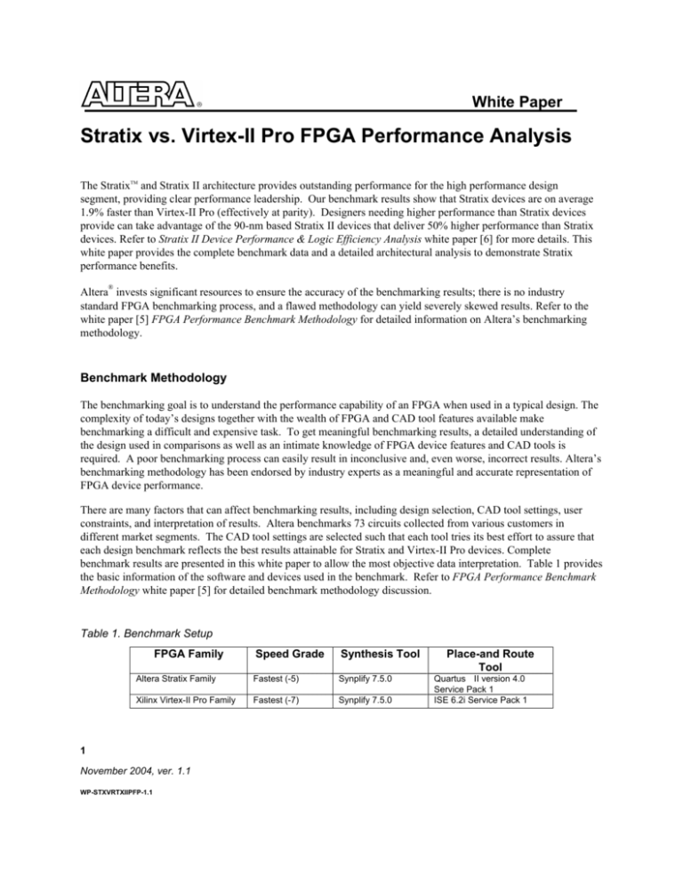
benchmark results are presented in this white paper to allow the most objective data interpretation. Table 1 provides
the basic information of the software and devices used in the benchmark. Refer to FPGA Performance Benchmark
Methodology white paper [5] for detailed benchmark methodology discussion.
Table 1. Benchmark Setup
FPGA Family
Speed Grade
Synthesis Tool
Altera Stratix Family
Fastest (-5)
Synplify 7.5.0
Xilinx Virtex-II Pro Family
Fastest (-7)
Synplify 7.5.0
1
November 2004, ver. 1.1
WP-STXVRTXIIPFP-1.1
Place-and Route
Tool
Quartus II version 4.0
Service Pack 1
ISE 6.2i Service Pack 1
Stratix vs. Virtex-II Pro FPGA Performance Analysis
Altera Corporation
Based on the benchmark results, the Stratix family shows an average of 1.9% performance advantage over Xilinx’s
Virtex-II Pro family. The performance advantage observed in Stratix devices is attributed to the combination of the
®
state-of-the-art algorithms in the Quartus II software and the advanced architecture and I/O interface support in
Stratix devices. For performance ratios in figures shown in this section, the followings apply:
• Performance ratio > 1 : Stratix device outperforms Virtex-II Pro device
• Performance ratio = 1 : Stratix and Virtex-II Pro devices show the same performance
• Performance ratio < 1 : Virtex-II Pro device outperforms Stratix device
Figure 1. Best-Effort Performance Benchmark Comparison Between Stratix and Virtex-II Pro Devices
As this result is significantly different from the performance results summarized in Xilinx white paper WP206 [8],
we will clearly highlight details for the benchmarking methodology and architectural differences. The
benchmarking methodology details are covered in FPGA Performance Benchmark Methodology white paper. The
architectural differences are discussed in the following sections.
Stratix FPGA Architectural Advantages
The following sections discuss the factors that significantly contribute to the success of the Stratix family. These
factors include:
•
•
•
•
•
2
Advanced EDA Tool - The Quartus II Software
Look-up Table (LUT) and Routing Resource Performance
Digital Signal Processing (DPS) Performance
Source Synchronous I/O Dedicated SERDES Support
Clock Network Resources
Altera Corporation
Stratix vs. Virtex-II Pro FPGA Performance Analysis
Advanced EDA Tool - The Quartus II Software
The Quartus II software’s state-of-the-art FPGA place-and-route engine takes full advantage of the Stratix family’s
architectural advancements and dedicated features to offer the performance needed in today’s sophisticated designs.
Xilinx white paper WP206 [8] refers to the UCLA study, “Optimality and Stability Study of Timing-Driven
Placement Algorithms” [1], which found that the Xilinx ISE placer was 4.1% from optimal. The same research has
shown that the Quartus II software is only 3.0% away from the optimal, setting the Quartus II software as the most
optimal FPGA place-and-route software in the industry. Xilinx collateral [8] omits this point and suggests that
Xilinx tools outperform other tools in the industry.
In addition to the leadership in the place-and-route engine, the Quartus II software’s timing analyzer performs
thorough timing analysis and handles many timing analysis pitfalls [3] to reduce the risk of a design failing due to
improper analysis. The Quartus II Design Space Explorer (DSE) and integrated physical synthesis technology
further strengthen the Quartus II leadership in the timing closure technology, allowing designers an automated
mechanism for obtaining the best performance for their systems in FPGAs.
Look-up Table and Routing Resource Performance
The factors used to determine maximum FPGA performance is a combination of the silicon fabrication process,
logic and routing structure, dedicated features, I/O support, and the maturity of the EDA tool. By examining the
equivalent micro timing parameters such as the look-up table (LUT), routing segments and dedicated feature, they
serve as indicators of how one FPGA architecture compares against another.
The Stratix LUT distinct attribute allows different propagation delay depending on which input is in use (See Figure
2). The Quartus II software automatically takes full advantage of this attribute and rotates inputs to the LUT such
that the critical path of a design can enjoy the fast path through the LUT. However according to Xilinx ISE 6.2i
software, the Virtex-II Pro LUT delay is the same for each of the inputs.
Figure 2. Stratix LUT vs. Virtex-II Pro LUT and Dedicated Multiplexer Delay Comparison
MUXF5
Fast Path
75ps
274ps
183ps
274ps
280ps
274ps
366ps
274ps
Stratix LUT Delay
1 Logic Level
Virtex-II Pro LUT Delay
1 Logic Level
324ps
324ps
483-539ps
Virtex-II Pro Dedicated
Multiplexer Delay
1 Logic Level
3
Stratix vs. Virtex-II Pro FPGA Performance Analysis
Altera Corporation
The Xilinx white paper WP209 [9] suggests that the dedicated two-input multiplexers (MUXF function expander)
in each slice can be used to implement wide functions and hence improve the performance, density and size of wide
logic functions. However, the delay of the MUXF is worse than the delay of the LUTs as shown in Figure 3; these
dedicated multiplexers in Virtex-II Pro devices provide no real improvement in the logic performance. Also, due to
the excessive delay from the MUXFs, each MUXF should be considered a distinct logic level, contrary to the Xilinx
white paper WP206 [8] which only considered LUTs as logic levels.
Figure 3. Stratix vs. Virtex-II Pro Logic Delay Comparison
4
Altera Corporation
Stratix vs. Virtex-II Pro FPGA Performance Analysis
Routing delay is also a reference point for determining the overall FPGA performance. The Stratix family is
designed to have an outstanding routing architecture to allow optimal speed and rout ability for a design. Figure 4
shows the result of an analysis on the routing delay versus distance between Stratix and Virtex-II Pro devices. The
Stratix family consistently shows better routing performance over the Virtex-II Pro family.
Figure 4. Path Delay vs. Distance Profile for Stratix and Virtex-II Pro Devices
Notes for Figure 4:
1. Stratix EP1S80 -5 speed grade and Virtex-II Pro XC2VP70 -7 speed grade are used
2. Stratix and Virtex-II Pro data are extracted from Quartus II version 4.0 service pack 1 and ISE 6.2i service pack 1, respectively
3. Delay is measured for the path between two registers without logic components (such as LUT, dedicated multiplexers, etc)
5
Stratix vs. Virtex-II Pro FPGA Performance Analysis
Altera Corporation
Digital Signal Processing Performance
The Stratix DSP blocks provide a superior solution over the Virtex-II Pro family’s simple multipliers in
performance. Stratix DSP blocks are more than simple multipliers; each DSP has configuration capabilities to
perform up to four 18x18-signed multiplication or two 18x18 multiply-and-accumulate (MAC) operations at 278
MHz.
For a simple non-pipelined 18x18 signed multiplier with its input and output signals registered, the Stratix DSP
block outperforms Virtex-II Pro by 21%. The Stratix DSP performance advantage increases further when the data
width of the multiplier or MAC function increases. For a non-pipelined, 36x36 signed multiplier, the Stratix DSP
block is 108% faster than Virtex-II Pro. Even after inserting seven pipeline stages, the maximum allowed by Xilinx
CoreGen, for a 36x36 signed multiplier, the Stratix DSP block with one pipeline stage still outperforms Virtex-II
Pro by 16%. See Figure 5.
Figure 5. Multiplier and MAC Performance Comparison between Stratix and Virtex-II Pro
Note for Figure 5:
1. Stratix design has only one pipeline stage and Virtex-II Pro design has seven-pipeline stages.
6
Altera Corporation
Stratix vs. Virtex-II Pro FPGA Performance Analysis
Source-Synchronous I/O Dedicated SERDES Support
Altera’s Stratix family provides dedicated serializer-deserializer (SERDES) for source-synchronous low voltage
differential signaling (LVDS) interface that is not available in Virtex-II Pro. The Stratix dedicated SERDES
optimized performance circuitry and its predictable timing provide the designer with a reliable implementation for
high speed, source-synchronous LVDS channels operating at up to 840Mb/s. In addition, the Quartus II
MegaWizard provides a user-friendly interface for designers to implement high-speed LVDS channels using the
dedicated SERDES circuitry See Figure 6.
Figure 6. Quartus MegaWizard for LVDS Instantiation
Xilinx application note XAPP265, High Speed Serialization and Deserialization (840Mb/s LVDS) [10], suggests a
solution that builds SERDES using Virtex-II or Virtex-II Pro’s internal logic. In order to meet the stringent timing
requirement, this reference design uses a substantial amount of manual placements which significantly restricts the
placement and routing of the custom logic surrounding the SERDES.
In addition to placement restrictions, this reference design consumes three of the eight global clocking buffers
(BUFGs) in a quadrant of a Virtex-II Pro device and hence, puts further constraints on the already scarce global
clock/signal resources.
7
Stratix vs. Virtex-II Pro FPGA Performance Analysis
Altera Corporation
Clock Network Resources
Modern FPGA designs often require many clocks to process data paths from different clock domains, with some of
these clocks being used throughout the entire design while some are used only in localized portions of it.
The Stratix clocking architecture supports a maximum of 64 dedicated, low-skew networks, allowing any particular
area of logic to have access to at least 22 unique clocks. The Xilinx Virtex-II Pro family provides a maximum of 16
dedicated chip-wide networks, and any particular area of logic has access to only eight of them, giving Stratix
designers access to four times as many dedicated low-skew networks, and nearly three times as many in any
particular area of the chip. See Figure 7.
Figure 7. Clock Network Resources Comparison between Stratix and Virtex-II Pro
In addition to providing easy-to-use access to more clocks, the Stratix architecture’s quadrant-wide and
octant-wide clock networks allow localized clocks to use a smaller dedicated network, resulting in significant power
savings in the clock network, a large consumer of dynamic power.
8
Altera Corporation
Stratix vs. Virtex-II Pro FPGA Performance Analysis
Conclusion
Our benchmark results indicate that the Stratix family offers similar system performance as Virtex-II Pro despite the
40% performance advantage claimed by Xilinx in WP206 [8]. In addition, the same academic research referenced
by Xilinx WP206 concluded that the Quartus II place-and-route engine produces outstanding results that are only
3% away from optimal on average. While there are many architectural features that provide benefits for specific
designs, both the Stratix architecture and the Virtex-II Pro architecture deliver excellent performance. This parity
summary is clearly very different from the conclusions drawn from Xilinx WP206, which used a biased and
incorrect methodology. For the highest performance, the Stratix II architecture delivers a 50% boost making it the
clear performance leader over both Stratix and Virtex-II Pro families. The new Stratix II architecture provides clear
performance leadership among all FPGAs.
For detailed information on the benchmarking methodology employed by Altera, refer to FPGA Performance
Benchmark Methodology white paper [5].
9
Stratix vs. Virtex-II Pro FPGA Performance Analysis
Altera Corporation
References
[1]
Cong J., Romesis M., and Xie M. Optimality and Stability Study of Timing-Driven Placement Algorithms,
UCLA Technical Report 030030. (http://cadlab.cs.ucla.edu/~michail/tpeko.pdf)
[2]
Altera Stratix Handbook
[3]
Altera white paper, “Performing Equivalent Timing Analysis between the Altera Quartus II Software and
Xilinx ISE”
[4]
Altera white paper, “The Benefits of Altera’s High-Speed DDR SDRAM Memory Interface Solution”
[5]
Altera white paper, “FPGA Performance Benchmark Methodology”
[6]
Altera white paper, “Stratix II Device Performance & Logic Efficiency Analysis”
[7]
Xilinx Data Sheet, DS083, “Virtex-II Pro Platform FPGAs Complete Data Sheet”, version 3.1, February
19, 2004
[8]
Xilinx white paper, WP206, “The 40% Performance Advantage of Virtex-II Pro FPGAs over Competitive
PLDs”, version 1.2, March 1, 2004
[9]
Xilinx white paper, WP209, “Virtex Variable-Input LUT Architecture”, version 1.0, January 12, 2004
[10]
Xilinx application note, XAPP265, “High Speed Serialization and Deserialization (840Mb/s LVDS)”,
version 1.3, June 19, 2002
Copyright © 2004 Altera Corporation. All rights reserved. Altera, The Programmable Solutions
Company, the stylized Altera logo, specific device designations, and all other words and logos
101 Innovation Drive
San Jose, CA 95134
(408) 544-7000
www.altera.com
that are identified as trademarks and/or service marks are, unless noted otherwise, the
trademarks and service marks of Altera Corporation in the U.S. and other countries.* All other
product or service names are the property of their respective holders. Altera products are
protected under numerous U.S. and foreign patents and pending applications, maskwork
rights, and copyrights. Altera warrants performance of its semiconductor products to current
specifications in accordance with Altera’s standard warranty, but reserves the right to make
changes to any products and services at any time without notice. Altera assumes no
responsibility or liability arising out of the application or use of any information, product, or
service described herein except as expressly agreed to in writing by Altera Corporation. Altera
customers are advised to obtain the latest version of device specifications before relying on
any published information and before placing orders for products or services.
10
