A 1.5GS/s 4096-Point Digital Spectrum Analyzer for Space
advertisement
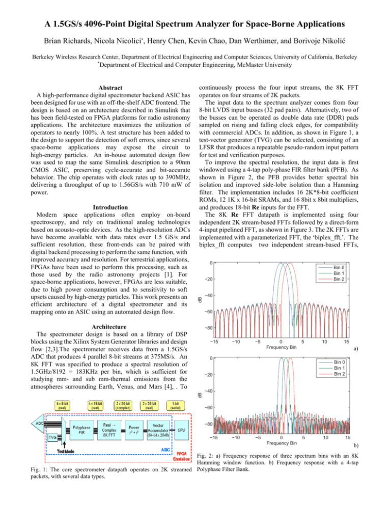
A 1.5GS/s 4096-Point Digital Spectrum Analyzer for Space-Borne Applications Brian Richards, Nicola Nicolici, Henry Chen, Kevin Chao, Dan Werthimer, and Borivoje Nikolić Berkeley Wireless Research Center, Department of Electrical Engineering and Computer Sciences, University of California, Berkeley Department of Electrical and Computer Engineering, McMaster University Introduction Modern space applications often employ on-board spectroscopy, and rely on traditional analog technologies based on acousto-optic devices. As the high-resolution ADCs have become available with data rates over 1.5 GS/s and sufficient resolution, these front-ends can be paired with digital backend processing to perform the same function, with improved accuracy and resolution. For terrestrial applications, FPGAs have been used to perform this processing, such as those used by the radio astronomy projects [1]. For space-borne applications, however, FPGAs are less suitable, due to high power consumption and to sensitivity to soft upsets caused by high-energy particles. This work presents an efficient architecture of a digital spectrometer and its mapping onto an ASIC using an automated design flow. continuously process the four input streams, the 8K FFT operates on four streams of 2K packets. The input data to the spectrum analyzer comes from four 8-bit LVDS input busses (32 pad pairs). Alternatively, two of the busses can be operated as double data rate (DDR) pads sampled on rising and falling clock edges, for compatibility with commercial ADCs. In addition, as shown in Figure 1, a test-vector generator (TVG) can be selected, consisting of an LFSR that produces a repeatable pseudo-random input pattern for test and verification purposes. To improve the spectral resolution, the input data is first windowed using a 4-tap poly-phase FIR filter bank (PFB). As shown in Figure 2, the PFB provides better spectral bin isolation and improved side-lobe isolation than a Hamming filter. The implementation includes 16 2K*8-bit coefficient ROMs, 12 1K x 16-bit SRAMs, and 16 8bit x 8bit multipliers, and produces 18-bit Re inputs for the FFT. The 8K Re FFT datapath is implemented using four independent 2K stream-based FFTs followed by a direct-form 4-input pipelined FFT, as shown in Figure 3. The 2K FFTs are implemented with a parameterized FFT, the ‘biplex_fft,’. The biplex_fft computes two independent stream-based FFTs, 0 Bin 0 Bin 1 Bin 2 −20 dB Abstract A high-performance digital spectrometer backend ASIC has been designed for use with an off-the-shelf ADC frontend. The design is based on an architecture described in Simulink that has been field-tested on FPGA platforms for radio astronomy applications. The architecture maximizes the utilization of operators to nearly 100%. A test structure has been added to the design to support the detection of soft errors, since several space-borne applications may expose the circuit to high-energy particles. An in-house automated design flow was used to map the same Simulink description to a 90nm CMOS ASIC, preserving cycle-accurate and bit-accurate behavior. The chip operates with clock rates up to 390MHz, delivering a throughput of up to 1.56GS/s with 710 mW of power. −40 −60 Architecture The spectrometer design is based on a library of DSP blocks using the Xilinx System Generator libraries and design flow [2,3].The spectrometer receives data from a 1.5GS/s ADC that produces 4 parallel 8-bit streams at 375MS/s. An 8K FFT was specified to produce a spectral resolution of 1.5GHz/8192 = 183KHz per bin, which is sufficient for studying mm- and sub mm-thermal emissions from the atmospheres surrounding Earth, Venus, and Mars [4], . To −80 −15 −10 −5 0 Frequency Bin 5 10 a) 0 Bin 0 Bin 1 Bin 2 −20 dB 15 −40 −60 −80 −15 −10 −5 0 Frequency Bin 5 10 15 b) Fig. 2: a) Frequency response of three spectrum bins with an 8K Hamming window function. b) Frequency response with a 4-tap Fig. 1: The core spectrometer datapath operates on 2K streamed Polyphase Filter Bank. packets, with several data types. a) b) Fig. 3: a) Computing S(f), the 8K FFT of s(t) from the Polyphase FIR filter. Note that 0 <= t < 2048, and b) Computing four Re to complex 2048-point FFTs using the stream-based biplex FFT. accepting two complex inputs and producing two complex outputs in every clock cycle. The four Re inputs can be combined so that a single biplex_fft datapath can compute all four 2K FFT calculations. The four Re input streams a(t), b(t), c(t), and d(t), are combined to produce the complex streams g(t) = a(t) + ib(t), and h(t) = c(t) + id(t). The biplex_fft then computes the FFTs G(f) and H(f) on every packet of N=2048 samples where 0 <= t < N, 0 <= f < N. G(f) and H(f) are scrambled in the output data streams, and must be re-ordered for later processing steps. Following the re-ordering operations, the reorder1/out is delayed by one cycle, aligning G(1) with G(N-1), G(2) with G(N-2), etc. These streams are combined, producing the first half of each spectrum: A(f) = (G(f)+G*(N-f)) / 2 B(f) = (G(f)-G*(N-f)) / 2 where 0 <= f < N/2, followed by C(F) = (H(f)+H*(N-f)) / 2 D(f) = (H(f)-H*(N-f)) / 2. where 0 <= f < N/2 as well. The cases where f = 0 and f = N/2 are exceptions, since G(0) = G(N), and G(N/2) = G(N-N/2). The Unscramble datapath handles the exceptions as special cases.. In addition, the Unscramble datapath exploits the property that A, B, C, and D have complex-conjugate symmetry, eg A(N-f) = A*(f), and only calculates the first N/2+1 points of each spectrum. The final stage is an SRAM-based mirroring (delay and time-reversal) block followed by a complex conjugate datapath that reconstructs the second half of each spectrum for N/2 < f < N. The Unscramble datapath area is dominated by SRAM blocks, required to perform the complex stream reordering operations.. 12 SRAM blocks implement delay, bit-reverse, time-reverse, and bit+time reverse blocks, and each single-port memory is continuously reading or writing. In the FPGA implementation, the architecture is optimized to exploit available dual-port SRAMs; in the ASIC implementation, only single-port SRAMs are being used, to reduce area and power. A direct-form FFT combines the four FFT’s A(f), B(f), C(f) and D(f) to produce the 8K FFT result as four streams of 2K packets. As with the 2K FFTs, the combined 8K FFT has even symmetry, allowing half of the frequency bins to be discarded by simply ignoring two of the direct-form FFT outputs. The two remaining output streams generate 4K complex frequency bins with 18-bit Re and 18-bit Im results, organized as two 2K packet streams. The power of the two complex streams is computed at the end of the signal processing chain, and the results are accumulated in the vector-accumulator block for a programmable number of packets. The vector-accumulator is essentially a 64-bit adder with feedback from a 2K x 64-bit synchronous delay line, thereby summing corresponding frequency bins from adjacent packets. The frequency data can thus be averaged over a period from 10ms to several seconds to trade-off the spectrum update time for improved SNR. Following the vector accumulator is a second set of SRAMs to buffer the accumulated results, preventing any loss of data while the spectrum is downloaded from the chip. A readout controller for a three-wire serial interface is provided to download the accumulated spectrum to an external processor. The serial data is transferred at less than 100 Mb/s, allowing single-ended LVTTL output pads to be chosen to reduce pin count. Test Architecture for Debugging and Soft-Upset Detection The spectrometer includes dedicated datapath elements to support testability and run-time soft-upset detection. The spectrometer supports two modes, “hard” and “soft.” In the hard mode, the spectrometer operation does not depend on any state registers, to prevent spectrometer failure caused by soft upsets from high-energy particles. The accumulation length is set to one of 16 values programmed through four (acc_length) input pins. a) b) Fig. 4: a) Scan testing architecture. b) MISR cell bit slice detail. In capture mode, the LSB cell in a multi-bit MISR is XORed with a characteristic polynomial like an LFSR to produce unique signatures. In the “soft” mode, these four inputs are re-defined to support internal testing modes. The accumulation length can be programmed to arbitrary values using “force” registers. Also, multiple-input shift registers (MISRs) are included to monitor streams of data at predetermined points between key function blocks. The MISR registers, shown in Figure 4, can generate unique signatures from streams of data during a preprogrammed interval. When combined with the internal test-vector generator, the same signature should recur unless a soft-upset changes one or more of the data values, effectively turning the entire spectrometer core area into a soft-upset detector. The MISR can also capture single-cycle data values to assist with debugging. The test results are accessible through the same three-wire serial interface used to read out the spectrum, eliminating the need for test-specific IOs. In addition to the MISR registers, the spectrometer includes a bypass mode to support debug and test. In bypass mode, the vector accumulator records raw input data and selected bits of intermediate datapath results. A 2K “snapshot” can be uploaded from the Vector Accumulator through the serial interface. Implementation and Measurements The complete system, including the test registers and controller, has been described in Simulink, and has been initially mapped to an FPGA and field tested. The same starting Simulink description has been translated and synthesized to an ASIC using a combination of commercial and in-house design tools [5]. By starting from the same high-level block diagram description and libraries used in several deployed FPGA applications, the turn-around time for designing and verifying the ASIC implementation is substantially reduced. The design flow optimizes for differences between FPGA and ASIC implementations by substituting datapath blocks with cycle-accurate and bit-accurate subsystems that may have different micro-architectures, as shown in Figure 5. For example, a memory-based synchronous delay line uses dual-port memories that have the same resource cost on an FPGA as a single-port memory. The same function would be inefficient on an ASIC, and is replaced by a single-port Fig. 5: A single description of the datapath is simulated in Simulink, compiled to an FPGA for emulation, and remapped to a cycle-accurate and bit-equivalent ASIC. Fig. 6: Die photo of the spectrometer ASIC. SRAM-based circuit that has the same I/O behavior. A Simulink testbench verifies equivalence by co-simulating the FPGA and ASIC implementations side-by-side. Using commercial synthesis, place and route tools in a custom ASIC flow, the design was mapped to a general-purpose 90nm 7M1P CMOS process, targeting a 375 MHz clock rate. Figure 6 shows the 2.8mm × 2.8mm ASIC, including double-row LVDS pads and a 2mm x 2mm core. The spectrometer ASIC is tested by using an FPGA test board programmed using the same design flow described previously. The design was fully tested at 200 MHz, limited by FPGA performance on the test board, with a core supply from 800mV to 1.4V, with core power consumption shown in Fig. 7. By using the built-in test vector generator, the maximum operating frequency was tested up to 390 MHz, consuming 670mW at 1V, with speed limited by IO bandwidth. The design specifications are summarized in Table 1. To test for vulnerability to soft upsets or latch-up from high-energy particles, the ASIC was tested using the 88” cyclotron[6]. The cyclotron produces high-energy ions that replicate the energy of particles found in space. A few seconds of testing with ions in the cyclotron mimics hours to weeks of soft-upset activity near a planet in space. In addition to varying the ion density, or fluence, the cyclotron can source ions of increasing mass from B to Xe, injecting energy at different depths within the substrate. To study soft upsets, the spectrometer is exercised using a synthetic input signal from the test vector generator, normally resulting in an unchanging frequency spectrum. Accumulated spectra are uploaded to the test FPGA board and compared with expected values. The Vcore a) Clock, MHz b) Fig. 7: Core power consumption (mA) at a) 200MHz, varying Vcore, and b) at 1V, varying the clock rate. Table 2: Soft upset impact on datapath, control, and accumulated spectra, based on MISR register scans. Table 1: Spectrometer Specifications Spec Description Clock Inputs LVDS, 375 MHz, tested to 390 MHz at 0.8V core ADC: 2x8-bit DDR LVDS 375 MHz or 4x8-bit SDR LVDS 375 MHz (1.5 GSPS Aggregate) 3-wire LVTTL serial readout 1.0V Core: 700mW, 375 MHz operation 2.5V LVDS and other I/O pads: 350mA 90nm CMOS STMicroelectronics, 2.8mm x 2.8mm 120 pin Ceramic PGA Output Supply Tech FPGA board then uploads erroneous spectra to a remote computer from which the experiment is controlled, for later processing. Figure 8 shows spectra corruption rates resulting from bombardment from a selection of ion sources and ion fluence rates. As expected, the spectrometer showed increasing errors as the ion density increased, with heavier ions resulting in more soft upsets. Also, longer accumulation periods resulted in a higher likelihood of finding a corrupt spectrum, and the design never latched-up. As the design presents a dataflow architecture, the spectra corruption differs depending on the part of the design where the upset happened. Qualitatively, the errors in the output spectra ranged from very small manifested in the non-essential parts to significant, as in Figure 9, which, however, happened rarely. A second series of experiments switched the spectrometer to soft mode so that the MISR registers could be monitored while exposing the spectrometer to ions. While reading the MISR registers, both datapath and control errors were observed. Datapath errors caused some MISR signatures to vary from expected values, indicating which subsystem was corrupted. Control errors resulted from reprogramming other registers in the scan chain or test controller. Table 2 shows a summary of the soft-mode experiments, showing that datapath and test control errors were much less frequent than errors in the accumulated spectra, suggesting that the Vector Accumulator subsystem was the most susceptible to soft upsets. This is expected, as the Vector Accumulator contains the largest amount of SRAM, that is the most vulnerable to upsets. One benefit of the FPGA-based testing methodology was the compact size of the test system, allowing it to fit easily into the cyclotron vacuum chamber. For operator safety, the test board had to be operated from a room 25 feet away from the device under test. Only minimal changes to the test setup were required, since standard Ethernet, serial, and BNC panels were available for the vacuum chamber. A conventional pattern Ion Fluence 1/cm2/sec Neon ~1000 Neon ~100 Krypton ~100 Spectra Errors 80/95 28/100 73/95 Datapath Errors 2 0 0 Control Errors 1 0 1 generator and logic analyzer would have been much more challenging to deploy at the testing facility due to increased size and cabling requirements. Conclusion A high-performance spectrum analyzer ASIC was designed by mapping a field-tested FPGA design to 90nm CMOS using an automated design flow, starting from the same high-level block-diagram description. The architecture included soft-upset testing and scan-chain-based debugging features. The chip was tested with high-energy ions to simulate the effect of alpha particles that the chip will be exposed to in space-borne applications. A majority of observed errors can be removed by using error correction in large SRAM arrays. Acknowledgements The authors acknowledge students, faculty and sponsors of BWRC, chip fabrication donation of STMicroelectronics, NSF Infrastructure Grant No. 0403427, C2S2, and support from Robert Jarnot and Paul Stek from NASA and JPL References [1] casper.berkeley.edu [2] www.mathworks.com. [3] Parsons, A., et al., "PetaOp/Second FPGA Signal Processing for SETI and Radio Astronomy," Asilomar Conference on Signals, Systems, and Computers, Nov 2006 [4] J.W. Waters, L. Froidevaux, R.F. Jarnot, et al, “An Overview of the EOS MLS Experiment,” Jet Propulsion Laboratory Document D-15745, Version 2.0, 2004. [5] D. Markovic, C. Chang, B. Richards, H. So, et al., "ASIC Design and Verification in an FPGA Environment," Proceedings Custom Integrated Circuits Conference (CICC'07), pp. 737-740, Sept 16-19, 2007, San Jose, CA. [6] cyclotron.lbl.gov 50 Isolated Error Normal TVG Spectrum 40 30 20 10 Error difference 0 0 Fig.8: Spectra error rate resulting from 10 MeV Boron and Argon ions. A new spectrum is calculated every 21ms. 500 1000 1500 2000 2500 3000 3500 4000 4500 Fig.9: Example of a corrupted TVG spectrum, on a log2 scale. Several small errors occur, and occasionally an isolated bin is corrupted.
