Logic Gates Lab: Breadboarding & Multisim - EET 1131
advertisement
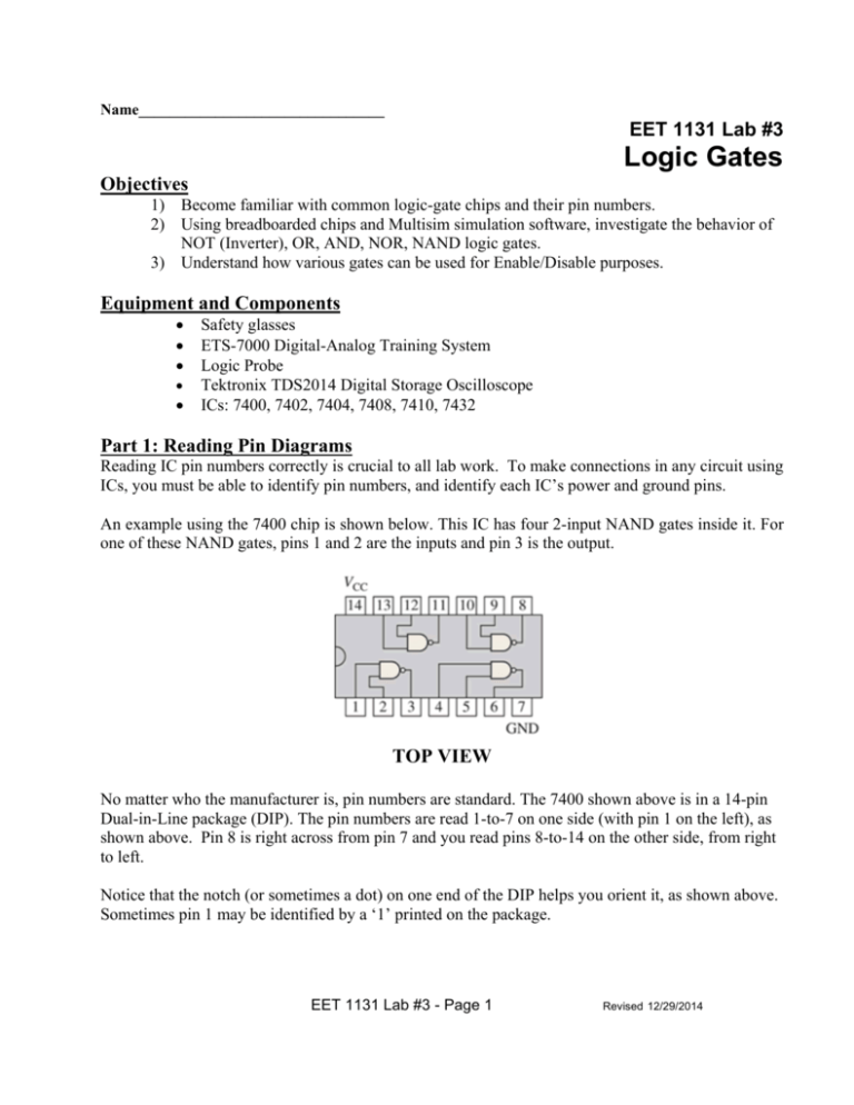
Name________________________________ EET 1131 Lab #3 Logic Gates Objectives 1) Become familiar with common logic-gate chips and their pin numbers. 2) Using breadboarded chips and Multisim simulation software, investigate the behavior of NOT (Inverter), OR, AND, NOR, NAND logic gates. 3) Understand how various gates can be used for Enable/Disable purposes. Equipment and Components Safety glasses ETS-7000 Digital-Analog Training System Logic Probe Tektronix TDS2014 Digital Storage Oscilloscope ICs: 7400, 7402, 7404, 7408, 7410, 7432 Part 1: Reading Pin Diagrams Reading IC pin numbers correctly is crucial to all lab work. To make connections in any circuit using ICs, you must be able to identify pin numbers, and identify each IC’s power and ground pins. An example using the 7400 chip is shown below. This IC has four 2-input NAND gates inside it. For one of these NAND gates, pins 1 and 2 are the inputs and pin 3 is the output. TOP VIEW No matter who the manufacturer is, pin numbers are standard. The 7400 shown above is in a 14-pin Dual-in-Line package (DIP). The pin numbers are read 1-to-7 on one side (with pin 1 on the left), as shown above. Pin 8 is right across from pin 7 and you read pins 8-to-14 on the other side, from right to left. Notice that the notch (or sometimes a dot) on one end of the DIP helps you orient it, as shown above. Sometimes pin 1 may be identified by a ‘1’ printed on the package. EET 1131 Lab #3 - Page 1 Revised 12/29/2014 (i) Using your textbook or Texas Instruments’ website (www.ti.com), draw gate symbols inside the IC outlines given below. Also label each pin with its pin number. 7400 7402 7404 7408 7432 7410 EET 1131 Lab #3 - Page 2 Revised 12/29/2014 Part 2: Testing Gates on the Breadboard [A] Inverters. 1. Place an inverter chip (7404) on the breadboard and provide it with power and ground. 2. Connect the first inverter’s input (labeled A below) to one of the trainer’s data switches. Connect the same inverter’s output (labeled X) to one of the trainer’s LEDs. 3. Test the inverter by observing the LED as you use the data switch to apply a HIGH (1) or a LOW (0) to the inverter’s input. Record your observations in Truth Table 1. Truth Table 1 Input Output A X 0 1 4. Ask me to check your work. Safety glasses? _________ Circuit works? ___________ DIP inserted correctly? __________ Using power/ground busses?__________ Wire colors? _________ Wire lengths? ___________Wire ends trimmed? ___________ DIP accessible? ___________ 5. You’re finished with this circuit and can take it apart. [B] AND Gates. 1. Place a 2-input AND chip (7408) on the breadboard. Connect pins 1 and 2 to two of the trainer’s data switches, and connect pin 3 to an LED. Then complete Truth Table 2. A 7408 EET 1131 Lab #3 - Page 3 Truth Table 2 X B 0 0 0 1 1 0 1 1 Revised 12/29/2014 2. With the trainer’s power turned off, disconnect the switch from one of your AND gate’s inputs, and connect this input to the trainer’s TTL MODE terminal instead, as shown below. Set the trainer’s function generator to produce a 1 kHz square wave at the TTL MODE terminal. To set your frequency accurately to 1 kHz, use the Fluke 45 to measure the frequency. Don’t rely on the labels next to the trainer’s Frequency knob. Display the TTL MODE signal on the oscilloscope’s Channel 1, and display output X on Channel 2. Don’t display Channels 3 and 4. Set each channel’s VOLTS/DIV setting to 5 V, and adjust the SEC/DIV control so that about four or five cycles of the waveforms are displayed. Below, use a straight-edge to draw the output X, first with the switch set High, and then with the switch set Low. If either output waveform is a flat line, label it as LOW or HIGH. TTL Mode Output X when Switch is High Output X when Switch is Low 3. Ask me to check your work. ___________ 4. In preparation for the next circuit, with the trainer’s power turned off, disconnect the TTL MODE from your AND gate’s input pin, and connect the input pin to a switch again. EET 1131 Lab #3 - Page 4 Revised 12/29/2014 5. In the diagram shown below, label each gate with its chip number and pin numbers. Then breadboard the circuit, test it using data switches and an LED, and complete Truth Table 3. A Truth Table 3 B 0 0 0 1 1 0 1 1 X 6. Ask me to check your work. Safety glasses? _________ Circuit works? ___________ DIPs inserted correctly? _________ Using power/ground busses?__________ Wire colors? _________ Wire lengths? ___________Wire ends trimmed? ___________ DIP accessible? ___________ 7. Take the circuit apart. [C] NAND Gates. 1. Label the gate shown below with its chip number and pin numbers. 2. Breadboard the gate, test it, and draw a complete truth table for it (Truth Table 4). EET 1131 Lab #3 - Page 5 Revised 12/29/2014 3. With the trainer’s power turned off, disconnect the switch from one of your NAND gate’s inputs, and connect this input to the trainer’s TTL MODE terminal instead, as shown below. Set the trainer’s function generator to produce a 25 kHz square wave at the TTL MODE terminal. To set your frequency accurately, use the Fluke 45 to measure the frequency. Don’t rely on the labels next to the trainer’s Frequency knob. Display the TTL MODE signal on the oscilloscope’s Channel 1, and display output X on Channel 2. Don’t display Channels 3 and 4. Set each channel’s VOLTS/DIV setting to 5 V, and adjust the SEC/DIV control so that about four or five cycles of the waveforms are displayed. Below, use a straight-edge to draw the output X, first with the switch set High, and then with the switch set Low. If either output waveform is a flat line, label it as LOW or HIGH. TTL Mode Output X when Switch is High Output X when Switch is Low 4. Ask me to check your work. ___________ 5. Take the circuit apart. EET 1131 Lab #3 - Page 6 Revised 12/29/2014 6. Draw the symbol for a 3-input NAND gate. Write the chip number and pin numbers on the symbol. 7. Now breadboard this gate, and test it using data switches and an LED. Draw a complete truth table for it (Truth Table 5). Then take your circuit apart. [D] OR Gates. 1. In the diagram shown below, label each gate with its chip number and pin numbers. 2. Breadboard the circuit, then test it using switches and an LED. Draw a complete truth table for it (Truth Table 6). 3. Ask me to check your work. Safety glasses? _________ Circuit works? __________ DIPs inserted correctly? __________ Using power/ground busses?__________ Wire colors? _________ Wire lengths? ___________Wire ends trimmed? ___________ DIPs accessible? ___________ EET 1131 Lab #3 - Page 7 Revised 12/29/2014 4. Build the circuit shown below. Set the trainer’s function generator to produce a 700 Hz square wave at the TTL MODE terminal. To set your frequency accurately, use the Fluke 45 to measure the frequency. Don’t rely on the labels next to the trainer’s Frequency knob. Display the TTL MODE signal on the oscilloscope’s Channel 1, and display output X on Channel 2. Don’t display Channels 3 and 4. Set each channel’s VOLTS/DIV setting to 5 V, and adjust the SEC/DIV control so that about four or five cycles of the waveforms are displayed. Below, use a straight-edge to draw the output X, first with the switch set High, and then with the switch set Low. If either output waveform is a flat line, label it as LOW or HIGH. TTL Mode Output X when Switch is High Output X when Switch is Low 5. Ask me to check your work. ___________ 6. Take the circuit apart. EET 1131 Lab #3 - Page 8 Revised 12/29/2014 [E] NOR Gates. 1. Label the gate shown below with its chip number and pin numbers. 2. Breadboard the gate, test it, and complete Truth Table 7. Then take your circuit apart. Truth Table 7 A B X [F] A More Complex Circuit 1. In the diagram below, label each gate with its chip number and pin numbers. 2. Breadboard the circuit, test it, and complete Truth Table 8. A Truth Table 8 B Z 3. Ask me to check your work. Safety glasses? _________ Circuit works? __________ DIPs inserted correctly? __________ Using power/ground busses?__________ Wire colors? _________ Wire lengths? ___________Wire ends trimmed? ___________ DIPs accessible? ___________ 4. You’re finished with this circuit and can take it apart. EET 1131 Lab #3 - Page 9 Revised 12/29/2014 Part 3: Testing Gates in Multisim In class you learned how to connect a logic gate for testing in Multisim. For example, shown below is a two-input AND gate connected to switches and an LED for testing, On the Lessons page of the course website is a folder named Unit 3 Multisim Files. This folder contains four Multisim files, and each file contains four gates. Your job is to test each gate and identify which gates are good and which gates are faulty. 1. Download AND_t-shoot_a.ms9 from the website and open it in Multisim. Identify each gate in this file as good or faulty: Gate U1A __________ Gate U1B ___________ Gate U1C ___________ Gate U1D ___________ 2. Do the same for the file named OR_t-shoot_a.ms9. Gate U1A __________ Gate U1B ___________ Gate U1C ___________ Gate U1D ___________ 3. Do the same for the file named NOR_t-shoot_a.ms9. Gate U1A __________ Gate U1B ___________ Gate U1C ___________ Gate U1D ___________ 4. Do the same for the file named NAND_t-shoot_a.ms9. Gate U1A __________ Gate U1B ___________ Gate U1C ___________ Gate U1D ___________ EET 1131 Lab #3 - Page 10 Revised 12/29/2014 Part 4: Review Questions. 1. How many NAND gates are there in one 7400 chip? ______ 2. How many NAND gates are there in one 7410 chip? ______ 3. Of the following four chips, which one is different from the other three in how the gates are laid out on the chip, and how would you describe this difference? 7400, 7402, 7408, and 7432 4. What are the pin numbers for VCC and GND connections on each chip you used? VCC = pin #__________ GND = pin #__________ 5. State in words how an AND gate works. Use complete sentences. 6. Suppose you didn’t have any 7402 chips, but you needed to build a circuit equivalent to one of the gates on a 7402. Which two chip numbers would you use? Draw a gate diagram showing how you would connect the gates from these two other chips. EET 1131 Lab #3 - Page 11 Revised 12/29/2014 7. Based on your observations in Step 2 of Part 2 [B], explain the “enable /disable” function of an AND gate. In other words, explain how an AND gate can be used to pass or stop data applied to one of its inputs. Use complete sentences. 8. NAND gates can also be used to perform an enable/disable function. Based on your observations in Step 3 of Part 2 [C], how is a NAND gate’s behavior similar to an AND gate’s behavior when both are used to perform the enable/disable function? How are they different? Use complete sentences. 9. OR gates can also be used to perform an enable/disable function. Based on your observations in Step 4 of Part 2 [D], how is an OR gate’s behavior similar to an AND gate’s behavior when both are used to perform the enable/disable function? How are they different? Use complete sentences. EET 1131 Lab #3 - Page 12 Revised 12/29/2014

