Vaibhav Gogte - Electrical Engineering and Computer Science
advertisement
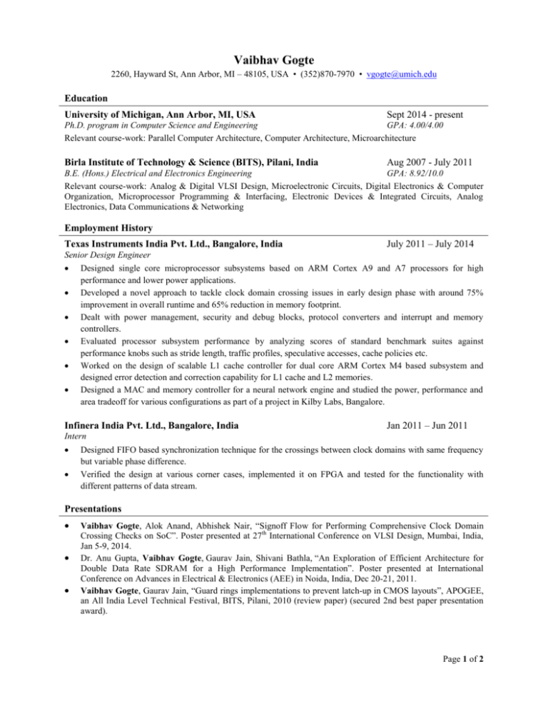
Vaibhav Gogte 2260, Hayward St, Ann Arbor, MI – 48105, USA • (352)870-7970 • vgogte@umich.edu Education University of Michigan, Ann Arbor, MI, USA Sept 2014 - present Ph.D. program in Computer Science and Engineering GPA: 4.00/4.00 Relevant course-work: Parallel Computer Architecture, Computer Architecture, Microarchitecture Birla Institute of Technology & Science (BITS), Pilani, India Aug 2007 - July 2011 B.E. (Hons.) Electrical and Electronics Engineering GPA: 8.92/10.0 Relevant course-work: Analog & Digital VLSI Design, Microelectronic Circuits, Digital Electronics & Computer Organization, Microprocessor Programming & Interfacing, Electronic Devices & Integrated Circuits, Analog Electronics, Data Communications & Networking Employment History Texas Instruments India Pvt. Ltd., Bangalore, India July 2011 – July 2014 Senior Design Engineer Designed single core microprocessor subsystems based on ARM Cortex A9 and A7 processors for high performance and lower power applications. Developed a novel approach to tackle clock domain crossing issues in early design phase with around 75% improvement in overall runtime and 65% reduction in memory footprint. Dealt with power management, security and debug blocks, protocol converters and interrupt and memory controllers. Evaluated processor subsystem performance by analyzing scores of standard benchmark suites against performance knobs such as stride length, traffic profiles, speculative accesses, cache policies etc. Worked on the design of scalable L1 cache controller for dual core ARM Cortex M4 based subsystem and designed error detection and correction capability for L1 cache and L2 memories. Designed a MAC and memory controller for a neural network engine and studied the power, performance and area tradeoff for various configurations as part of a project in Kilby Labs, Bangalore. Infinera India Pvt. Ltd., Bangalore, India Jan 2011 – Jun 2011 Intern Designed FIFO based synchronization technique for the crossings between clock domains with same frequency but variable phase difference. Verified the design at various corner cases, implemented it on FPGA and tested for the functionality with different patterns of data stream. Presentations Vaibhav Gogte, Alok Anand, Abhishek Nair, “Signoff Flow for Performing Comprehensive Clock Domain Crossing Checks on SoC”. Poster presented at 27th International Conference on VLSI Design, Mumbai, India, Jan 5-9, 2014. Dr. Anu Gupta, Vaibhav Gogte, Gaurav Jain, Shivani Bathla, “An Exploration of Efficient Architecture for Double Data Rate SDRAM for a High Performance Implementation”. Poster presented at International Conference on Advances in Electrical & Electronics (AEE) in Noida, India, Dec 20-21, 2011. Vaibhav Gogte, Gaurav Jain, “Guard rings implementations to prevent latch-up in CMOS layouts”, APOGEE, an All India Level Technical Festival, BITS, Pilani, 2010 (review paper) (secured 2nd best paper presentation award). Page 1 of 2 Dr. H.D. Mathur, Vaibhav Gogte, Gaurav Jain, M. Geeth Kiran, “A Critical Review on Technical Aspects of Distributed Generation”, International Conference on Advances in Renewable Energy, MANIT, Bhopal, India, June 24-26, 2010. Major Projects Design, simulation and analysis of double data rate (DDR) memory architectures. o Designed DDR1 and DDR2 memory architectures and compared the designs in terms of performance throughput, power dissipation and hardware complexity Study and analysis of orthogonal frequency division multiplexing (OFDM) technology. o Simulated the OFDM based transmitter, receiver and channel in MATLAB and compared bit-error rate of the model with that of the BPSK modulation technique. Simulation of islanding detection techniques for distributed generation. o Islanding detection time was evaluated and compared for the active and passive anti-islanding techniques for distributed generation using MATLAB Simulink. Design of a fully pipelined CORDIC Processor for OFDM based WLAN. o Designed an iterative solution for trigonometric computations in Verilog HDL, synthesized the design and placed and routed it through semi-custom flow followed by verification of post-layout netlist. Design of two stage operational amplifier. o Implemented a two-stage operational amplifier in TSMC 180nm technology followed by a full-custom layout design. Teaching Experience Microelectronic Circuits, BITS-Pilani, India Circuits and Signals, BITS-Pilani, India Aug 2010 – Dec 2010 Jan 2010 – May 2010 Skill Set Computer Languages: CAD Tools: Software Packages: Operating Systems: C, C++, Python, Verilog, Assembly level programming of x86 and ARM v7-A processors, SPICE, Perl, Tcl. Cadence RC Compiler, Conformal LEC, Cadence NCSim, Code Composer Studio, PrimeTime, ModelSim, SoC Encounter, Virtuoso Analog Environment. MATLAB, Simulink, AutoCAD. Windows, Linux. Page 2 of 2

