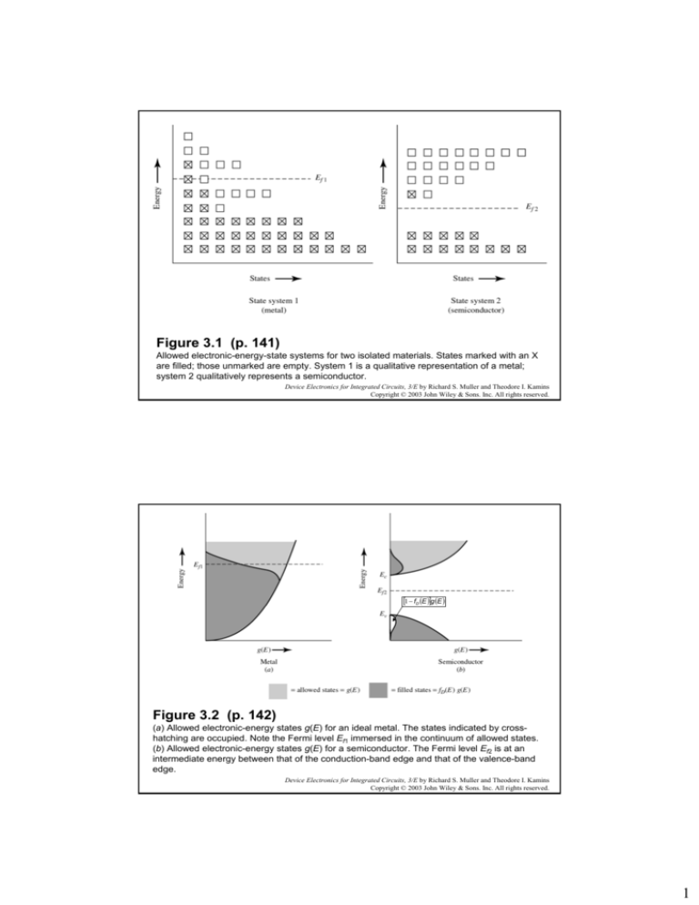
Figure 3.1 (p. 141)
Allowed electronic-energy-state systems for two isolated materials. States marked with an X
are filled; those unmarked are empty. System 1 is a qualitative representation of a metal;
system 2 qualitatively represents a semiconductor.
Device Electronics for Integrated Circuits, 3/E by Richard S. Muller and Theodore I. Kamins
Copyright © 2003 John Wiley & Sons. Inc. All rights reserved.
[1 − fD (E )]g (E )
Figure 3.2 (p. 142)
(a) Allowed electronic-energy states g(E) for an ideal metal. The states indicated by crosshatching are occupied. Note the Fermi level Ef1 immersed in the continuum of allowed states.
(b) Allowed electronic-energy states g(E) for a semiconductor. The Fermi level Ef2 is at an
intermediate energy between that of the conduction-band edge and that of the valence-band
edge.
Device Electronics for Integrated Circuits, 3/E by Richard S. Muller and Theodore I. Kamins
Copyright © 2003 John Wiley & Sons. Inc. All rights reserved.
1
qΦM
Figure 3.3 (p. 142)
Pertinent energy levels for the metal gold and the semiconductor silicon. Only the work
function is given for the metal, whereas the semiconductor is described by the work function
qΦs, the electron affinity qXs, and the band gap (Ec – Ev).
Device Electronics for Integrated Circuits, 3/E by Richard S. Muller and Theodore I. Kamins
Copyright © 2003 John Wiley & Sons. Inc. All rights reserved.
Figure 7.2.
(a) Energy band
diagram of an
isolated metal
adjacent to an
isolated n-type
semiconductor
under thermal
nonequilibrium
condition. (b)
Energy band
diagram of a
metalsemiconductor
contact in
thermal
equilibrium.
qΦM
q(ΦM-χ)
Device Electronics for Integrated Circuits, 3/E by Richard S. Muller and Theodore I. Kamins
Copyright © 2003 John Wiley & Sons. Inc. All rights reserved.
2
Figure 3.4 (p. 144)
(a) Idealized equilibrium band diagram
(energy versus distance) for a metalsemiconductor rectifying contact
(Schottky barrier). The physical
junction is at x = 0. (b) Charge at an
idealized metal-semiconductor
junction. The negative charge is
approximately a delta function at the
metal surface. The positive charge
consists entirely of ionized donors
(here assumed constant in space) in
the depletion approximation. (c) Field
at an idealized metal-semiconductor
junction.
E
Emax
Device Electronics for Integrated Circuits, 3/E by Richard S. Muller and Theodore I. Kamins
Copyright © 2003 John Wiley & Sons. Inc. All rights reserved.
Figure 3.5 (p. 146)
Idealized band diagrams (energy versus distance) at a metal-semiconductor junction (a)
under applied forward bias (Va > 0) and (b) under applied reverse bias (Va < 0). The
semiconductor is taken as the reference (voltage ground) as shown in (c). The vacuum
levels for the two cases are not shown.
Device Electronics for Integrated Circuits, 3/E by Richard S. Muller and Theodore I. Kamins
Copyright © 2003 John Wiley & Sons. Inc. All rights reserved.
3
Figure 7.7. Current transport by the thermionic emission process.
(a) Thermal equilibrium; (b) forward bias; and (c) reverse bias.5
Device Electronics for Integrated Circuits, 3/E by Richard S. Muller and Theodore I. Kamins
Copyright © 2003 John Wiley & Sons. Inc. All rights reserved.
2
qε Si ND
Figure 3.6 (p. 147)
Devicefor
Electronics
for Integrated
Circuits, 3/E by Richard
S. Muller and Theodore I. Kamins
Plot of 1/C2 versus applied voltage
an ideal
metal-semiconductor
junction.
Copyright © 2003 John Wiley & Sons. Inc. All rights reserved.
4
Figure 7.6.
1/C2 versus
applied voltage
for W-Si and
W-GaAs
diodes.
Device Electronics for Integrated Circuits, 3/E by Richard S. Muller and Theodore I. Kamins
Copyright © 2003 John Wiley & Sons. Inc. All rights reserved.
Figure 3.7 (p. 148)
Schematic representation of space charge at a metal-semiconductor junction with nonuniform
doping in the semiconductor.
Device Electronics for Integrated Circuits, 3/E by Richard S. Muller and Theodore I. Kamins
Copyright © 2003 John Wiley & Sons. Inc. All rights reserved.
5
Figure 7.8.
Forward current
density versus
applied voltage of
W-Si and W-GaAs
diodes.4
Device Electronics for Integrated Circuits, 3/E by Richard S. Muller and Theodore I. Kamins
Copyright © 2003 John Wiley & Sons. Inc. All rights reserved.
Device Electronics for Integrated Circuits, 3/E by Richard S. Muller and Theodore I. Kamins
Copyright © 2003 John Wiley & Sons. Inc. All rights reserved.
6
Example: Schottky Barrier Diode (p. 149)
Device Electronics for Integrated Circuits, 3/E by Richard S. Muller and Theodore I. Kamins
Copyright © 2003 John Wiley & Sons. Inc. All rights reserved.
Example: Schottky Barrier Diode (cont., p. 150)
Device Electronics for Integrated Circuits, 3/E by Richard S. Muller and Theodore I. Kamins
Copyright © 2003 John Wiley & Sons. Inc. All rights reserved.
7
Figure 3.8 (p. 151)
Classical energy diagram for a free electron near a plane metal surface at thermal
equilibrium [E1(x)], and with an applied field –ξ [E2(x)].
Device Electronics for Integrated Circuits, 3/E by Richard S. Muller and Theodore I. Kamins
Copyright © 2003 John Wiley & Sons. Inc. All rights reserved.
Figure 3.9 (p. 154)
(a) Band diagram of a rectifying metal-semiconductor junction under forward bias. The
applied voltage Va displaces the Fermi levels: qVa = Efs – Efm. (b) The potential across the
surface depletion layer is decreased to Φi – Va.
Device Electronics for Integrated Circuits, 3/E by Richard S. Muller and Theodore I. Kamins
Copyright © 2003 John Wiley & Sons. Inc. All rights reserved.
8
Figure 3.10 (p. 156)
Measured values of current (plotted
on a logarithmic scale) versus
voltage for an aluminum-silicon
Schottky barrier. Values for Is = JśA
and n are obtained from an empirical
fit of the data to Equation 3.3.17.
Device Electronics for Integrated Circuits, 3/E by Richard S. Muller and Theodore I. Kamins
Copyright © 2003 John Wiley & Sons. Inc. All rights reserved.
Figure 3.12 (p. 159)
Metal-semiconductor barrier with a thin space-charge region through which electrons can
tunnel. (a) Tunneling from metal to semiconductor. (b) Tunneling from semiconductor to
metal.
Device Electronics for Integrated Circuits, 3/E by Richard S. Muller and Theodore I. Kamins
Copyright © 2003 John Wiley & Sons. Inc. All rights reserved.
9
Figure 3.13a (p. 160)
(a) An idealized equilibrium energy diagram for a Schottky ohmic contact between a metal
and an n-type semiconductor.
Device Electronics for Integrated Circuits, 3/E by Richard S. Muller and Theodore I. Kamins
Copyright © 2003 John Wiley & Sons. Inc. All rights reserved.
Figure 3.13b (p. 160)
(b) Charge at an ideal Schottky ohmic contact. A delta function of positive charge at the
metal surface couples to a distributed excess-electron density n’(x) in the semiconductor.
Device Electronics for Integrated Circuits, 3/E by Richard S. Muller and Theodore I. Kamins
Copyright © 2003 John Wiley & Sons. Inc. All rights reserved.
10
Figure 3.13b (p. 160)
(c) Field.
Device Electronics for Integrated Circuits, 3/E by Richard S. Muller and Theodore I. Kamins
Copyright © 2003 John Wiley & Sons. Inc. All rights reserved.
Figure 3.13c (p. 160)
(d) Potential at an idealized Schottky ohmic contact. The Debye length LD is a characteristic
measure of the extent of the charge and field.
Device Electronics for Integrated Circuits, 3/E by Richard S. Muller and Theodore I. Kamins
Copyright © 2003 John Wiley & Sons. Inc. All rights reserved.
11
Figure 3.14 (p. 162)
Bonding diagram for a silicon crystal near its surface (straight lines indicate coupled pairs of
bonding electrons). The bonds at a clean semiconductor surface are anistropic and,
consequently, the allowed energy levels differ from those in the bulk.
Device Electronics for Integrated Circuits, 3/E by Richard S. Muller and Theodore I. Kamins
Copyright © 2003 John Wiley & Sons. Inc. All rights reserved.
Figure 3.15 (p. 163)
Approximate distribution of
Tamm-Schockley states in the
diamond lattice [8]. The
distribution appears to peak
sharply at an energy roughly onethird of the bandgap above Ev.
Device Electronics for Integrated Circuits, 3/E by Richard S. Muller and Theodore I. Kamins
Copyright © 2003 John Wiley & Sons. Inc. All rights reserved.
12
Figure 3.16 (p. 164)
Band structure near a metal-semiconductor contact according to the model of Cowley and
Sze [9]. The model considers a thin interfacial layer of thickness Ê that sustains a voltage ∆
at equilibrium. Acceptor-type surface states distributed in energy are assumed to be
described by a distribution function Ds states cm-2 eV-1.
Device Electronics for Integrated Circuits, 3/E by Richard S. Muller and Theodore I. Kamins
Copyright © 2003 John Wiley & Sons. Inc. All rights reserved.
Figure 3.17 (p. 165)
Band diagram for a semiconductor surface showing a thin surface layer containing acceptortype surface sates distributed in energy. A surface-depletion region is present because of
charge in the surface states.
Device Electronics for Integrated Circuits, 3/E by Richard S. Muller and Theodore I. Kamins
Copyright © 2003 John Wiley & Sons. Inc. All rights reserved.
13
Figure 3.18 (p. 167)
Schottky-barrier-gate, field-effect transistor. Current ID flowing from drain to source is
modulated by gate voltage VG that controls the dimensions of the depletion region. This, in
turn, modulates the cross-sectional conducting area for ID. The source and drain contacts
are ohmic because they are made to highly doped material.
Device Electronics for Integrated Circuits, 3/E by Richard S. Muller and Theodore I. Kamins
Copyright © 2003 John Wiley & Sons. Inc. All rights reserved.
Figure 3.19 (p. 167)
Special processing techniques improve the performance of Schottky diodes shown here in
cross section. (a) The diffused p-type guard ring leads to a uniform electric field and
eliminates breakdown at the junction edges and corners. (b) The metal field plate is an
alternative means for achieving the same effect.
Device Electronics for Integrated Circuits, 3/E by Richard S. Muller and Theodore I. Kamins
Copyright © 2003 John Wiley & Sons. Inc. All rights reserved.
14
Figure 3.20 (p. 168)
Linear plot of current versus voltage for a Schottky diode illustrating the concept of a diode
“turn-on voltage.”
Device Electronics for Integrated Circuits, 3/E by Richard S. Muller and Theodore I. Kamins
Copyright © 2003 John Wiley & Sons. Inc. All rights reserved.
Figure 3.21 (p. 170)
Diagrams for ideal metal-semiconductor Schottky diodes.
Device Electronics for Integrated Circuits, 3/E by Richard S. Muller and Theodore I. Kamins
Copyright © 2003 John Wiley & Sons. Inc. All rights reserved.
15
