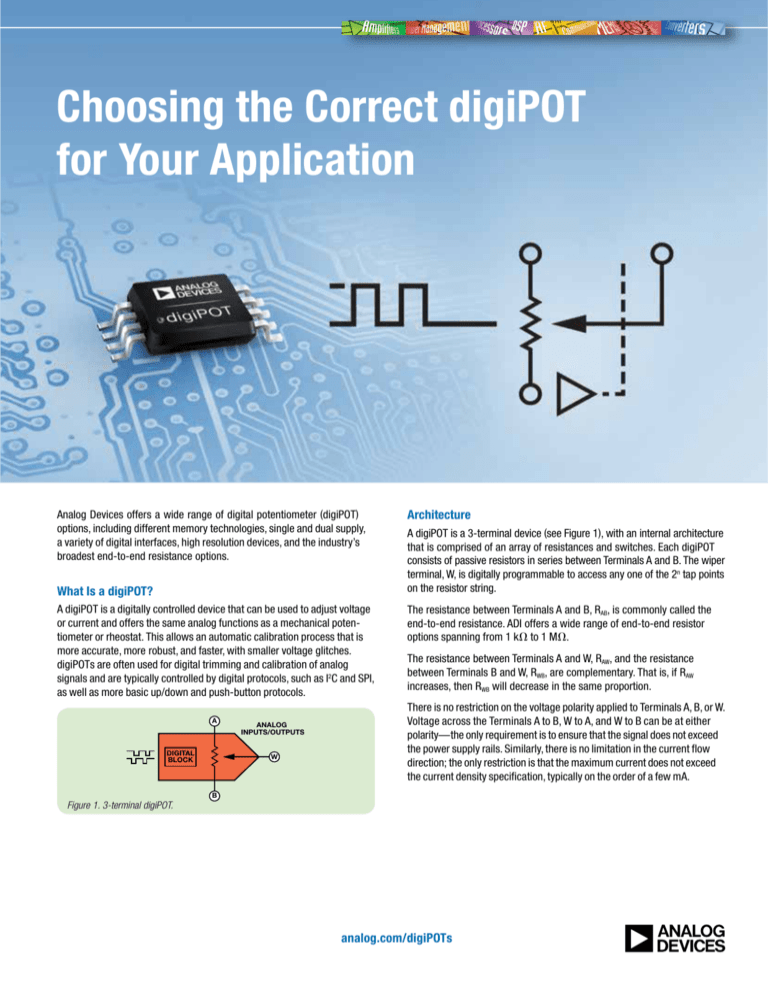
Choosing the Correct digiPOT
for Your Application
Analog Devices offers a wide range of digital potentiometer (digiPOT)
options, including different memory technologies, single and dual supply,
a variety of digital interfaces, high resolution devices, and the industry’s
broadest end-to-end resistance options.
What Is a digiPOT?
A digiPOT is a digitally controlled device that can be used to adjust voltage
or current and offers the same analog functions as a mechanical potentiometer or rheostat. This allows an automatic calibration process that is
more accurate, more robust, and faster, with smaller voltage glitches.
digiPOTs are often used for digital trimming and calibration of analog
signals and are typically controlled by digital protocols, such as I2C and SPI,
as well as more basic up/down and push-button protocols.
A
DIGITAL
BLOCK
Figure 1. 3-terminal digiPOT.
ANALOG
INPUTS/OUTPUTS
W
Architecture
A digiPOT is a 3-terminal device (see Figure 1), with an internal architecture
that is comprised of an array of resistances and switches. Each digiPOT
consists of passive resistors in series between Terminals A and B. The wiper
terminal, W, is digitally programmable to access any one of the 2n tap points
on the resistor string.
The resistance between Terminals A and B, RAB, is commonly called the
end-to-end resistance. ADI offers a wide range of end-to-end resistor
options spanning from 1 kΩ to 1 MΩ.
The resistance between Terminals A and W, RAW, and the resistance
between Terminals B and W, RWB, are complementary. That is, if RAW
increases, then RWB will decrease in the same proportion.
There is no restriction on the voltage polarity applied to Terminals A, B, or W.
Voltage across the Terminals A to B, W to A, and W to B can be at either
polarity— the only requirement is to ensure that the signal does not exceed
the power supply rails. Similarly, there is no limitation in the current flow
direction; the only restriction is that the maximum current does not exceed
the current density specification, typically on the order of a few mA.
B
analog.com/digiPOTs
Which digiPOT to Use?
Typical Applications
When choosing the correct digital potentiometer for your application,
the key parameters to consider are
• Wheatstone bridge calibration
I. Resistor configuration
V. End-to-end resistance
II. Digital interface
VI.Resolution
III. Internal memory
VII. Performance
IV.Supply voltage
VIII.Package
• Op amp gain control (see Figure 5)
• Analog filter tuning
A
A
A digiPOT can be configured as a potentiometer or as a rheostat.
Potentiometer Mode
In this configuration, there are three terminals available: A, B, and W
(see Figure 2).
The digiPOT operates as a voltage divider, and the wiper terminal voltage
is proportional to the voltage applied between the A and B terminals and
the resistance at RAW and RWB.
In Figure 3, a reference voltage is connected to Terminal A, and Terminal B
is grounded. The voltage at the wiper pin can be calculated as
VOUT =
CODE
2n
VOUT
A
W
I. Resistor Configuration
VIN
W
× VREF
R
W
B
RHEOSTAT
B
Figure 4. Rheostat.
Figure 5. Noninverting amplifier.
II. Digital Interface
ADI’s large digiPOT portfolio supports a wide range of digital interfaces:
• SPI — ADI offers SPI-compatible interfaces that can be operated at
speeds up to 50 MHz clock rate.
• I2C — ADI offers I2C-compatible interfaces that support standard and
fast mode, up to a 400 kHz clock rate. Address pins are typically
available, which allow the user to configure the slave address so that
multiple devices can be operated on the same bus.
• Push-Button — the user can interact directly with the system by just
adding two push-button switches. Press the UP button to increment
the resistance and DOWN to decrement resistance (see Figure 6).
Typical Applications
• DAC
• LCD VCOM adjustment
• Analog signal attenuation
VREF
• Up/Down — this is a simple interface, which can be operated by any
host controller or discrete logic or manually with a rotary encoder
or push buttons. With a single edge, resistance can be increased or
decreased.
A
VDD
W
B
UP
BUTTON
PU
Figure 2. Potentiometer.
Figure 3. DAC mode.
R
R
PD
DOWN
BUTTON
Rheostat Mode
The digiPOT can operate as a digitally controlled rheostat where only two
terminals are used. The unused terminal can be left floating or tied to the
W terminal, as shown in Figure 4.
The nominal end-to-end resistance (RAB) of the digiPOT has 2n contact
points accessible by the wiper terminal, and the resulting resistance can
be measured either across the wiper and B terminals (RWB) or across the
wiper and A terminals (RAW).
Figure 6. Push-button interface.
III. Internal Memory
The minimum wiper resistance is at the wiper’s first connection at the
B terminal for zero scale. This B terminal connection has a minimum
wiper contact resistance, RW, of typically 70 Ω.
ADI’s wide portfolio supports four different options of integrated memory,
allowing the user the flexibility to select the ideal digiPOT for the end
application. Internal memory allows the user to set the wiper’s power-on
reset (POR) position to a user programmed value. The wiper position can
be reprogrammed multiple times but always returns to the programmed
position on power-up. This function is ideal for calibration or for
applications that require a fast power-on time.
The rheostat resistance can be calculated by
• Volatile memory only: digiPOT typically powers up to midscale.
RAW =
2n – CODE
2n
× RAB + RW or RWB =
CODE
2n
× RAB + RW
• One-time programmable (OTP): allows user to program the wiper
power-up position once — ideal for factory calibration.
• Multitime programmable (MTP): ADI has product offerings that support
2×, 20×, or 50× programmable wiper memory.
• EEPROM: ADI’s integrated EEPROM offers endurance up to 1M
programming cycles and data retention of 50 years at 125°C.
IV. Supply Voltage
VII. Key Performance Parameters
Before selecting a digiPOT for an application, it is important to understand the maximum signal voltage that will be applied to the A, B, or
W terminals. The positive, VDD, and negative, VSS (or GND for a unipolar
digiPOT), power supplies define the voltage signal boundary conditions.
Signals that exceed VDD or VSS are typically clamped by internal forwardbiased diodes.
Resistor Tolerance Error — digiPOT resistor tolerance error is the
absolute end-to-end resistance error. This error is typically ±20% and
can be a critical parameter if matching to an external discrete resistor or
sensor in an open-loop application.
Reducing the Impact of Resistor Tolerance Error
• ADI offers digiPOTs, for example, the AD5272 and AD5292, with
industry-leading maximum ±1% variable resistor performance.
These devices enable designers to digitally program accurate resistor values, simplifying the process of determining the system error
budget (see Figure 9).
ADI’s large portfolio supports a wide range of supply options:
• Single supply: 2.3 V to 33 V (see Figure 7)
• Dual supply: ±2.25 V to ±16.5 V (see Figure 8)
• Low resistor tolerance, for example, the AD5110, with a ±1% typical
and ±8% maximum resistor tolerance.
VIN
+VDD
A
VIN
W
VOUT
0V
• Products such as the AD5259 and AD5235 have the resistor tolerance
error stored in the EEPROM memory. This allows the user to calculate
the actual end-to-end resistance to an accuracy of 0.01%.
VOUT
VOFFSET
0V
B
VOFFSET
• The new patented linear gain setting mode allows controlling the
potentiometer as two independent rheostats, RAW and RWB, connected
in a single point, W terminal (see Figure 10). This mode is ideal in
equations where the output depends on the ratio of two resistors,
G = R1/R2, for example, in an inverting amplifier. This mode can be
found in the AD5141, offering a maximum ratio error below ±1%.
Figure 7. AC signal, single-supply mode.
VIN
A
+VDD
+VDD
VIN
0V
W
–VSS
VOUT
0V
VOUT
–VSS
B
4
+IN
RDAC
Figure 8. AC signal, dual-supply mode.
RG IN-AMP
–IN
V. End-to-End Resistance
VREF
GAIN = 1 +
ADI offers a wide range of end-to-end resistor options, from 1 kΩ to
1 MΩ. This simplifies the task of achieving the optimum impedance,
power dissipation, bandwidth, and noise performance combination.
Resistance (𝛀)
1k 2.5k 5k
Resolution (Taps)
32
•
128
1024
10k 20k 25k 50k 80k 100k 200k 250k 1M
•
•
•
•
•
•
•
•
•
•
•
•
•
•
•
•
•
•
•
•
•
•
•
2
1
0
0
200 400 600 800 1000
DECIMAL CODE
ENABLE
RDAC
REGISTER
AW
A
A
RAW
RAW
RAW = RAB – RWB
W
Table 1. Quick Reference Resistance Options
•
RG
DISABLE
ADI has offerings ranging from 5-bit to 10-bit resolution offering LSB step
sizes as low as 4 Ω. If more resolution is required, then a cascade, serial,
or parallel combination of digiPOTs can be implemented (see Table 1).
256
49.400
3
Figure 9. Instrumentation amplifier.
VI. Resolution
64
VOUT
ERROR (%)
+VDD
VOFFSET
RDAC
REGISTER
WB
B
RAB = RAW + RWB
RWB
RDAC
REGISTER
WB
W
B
RWB
Figure 10. Linear gain setting mode.
•
•
•
digiPOT Temperature Coefficient — ADI’s digiPOTs leverage proprietary
thin film resistor technology, leading to the lowest temperature coefficient
performance available on the market (for example, AD5292):
• 5 ppm/°C in potentiometer mode
• 35 ppm/°C in rheostat mode
Bandwidth — the digiPOT architecture is comprised of resistors and
switches (see Figure 11). The resistance of the resistors in the path of a
particular code, combined with the switch parasitic, pin, and board capacitances, creates an RC low-pass filter, which determines the maximum ac
frequency that can be passed through the digiPOT before it is attenuated by
more than –3 dB. Choosing a low end-to-end resistor option will support a
higher –3 dB bandwidth (see Table 2).
Applications
AUDIO_INPUT
PUSH-UP
BUTTON
PU
PD
PUSH-DOWN
BUTTON
A
W
–
B
+
Table 2. Typical –3 dB Bandwidth vs. Resistor Option
Resistance
1 kΩ
5 kΩ
10 kΩ
50 kΩ
100 kΩ
1 MΩ
Frequency
5 MHz
2 MHz
1 MHz
120 kHz
70 kHz
6 kHz
Figure 13. Audio volume control with an amplifier and push-button interface.
VIN
SA
RL
VDD
+15V
A
RL
SW
SERIAL
INTERFACE
AD5292
A
W
RS
VOUT
B
W
SB
RS
GND
–15V
Figure 14. Logarithmic pro audio volume control.
RL
B
VSS
RL
Figure 11. Internal architecture.
THD — an ac signal applied to the terminals of a digiPOT will cause
variation in the internal switch, RON, leading to some nonsymmetrical
attenuation and, therefore, signal distortion (see Figure 12). Choosing a
high end-to-end resistor option reduces the contribution of the internal
switches’ resistance vs. the total resistance, leading to better THD
performance. Table 3 shows some typical THD performance values.
VIN
VOUT
Figure 15. Variable low-pass Sallen-Key filter.
Table 3. Typical THD Performance of the AD5292
Resistance
20 kΩ
50 kΩ
100 kΩ
THD
–93 dB
–101 dB
–106 dB
SIGNAL DISTORTION
INPUT SIGNAL
PMOS
VOUT
VIN
SERIAL
INTERFACE
NMOS
ATTENUATION
IDEAL OUTPUT SIGNAL
REAL OUTPUT SIGNAL
Figure 16. Programmable voltage source with current booster.
Figure 12. Total harmonic distortion.
VIII. Packages
ADI digiPOTs are available in a wide range of packages:
• SC70
• MSOP
• LFCSP
• TSSOP
• SOT-23
• SOIC
Reference circuit designs are engineered and tested for quick
and easy system integration to help solve today’s relevant design
challenges.
Visit the circuit library where you can find digiPOT circuit designs
at www.analog.com/circuits.
Nonvolatile Memory Digital Potentiometers
Part Number
Resolution
(Number of Wiper Steps)
One Time Programmable Memory (OTP)
AD5273
64
AD5171
64
AD5172
256
AD5173
256
Multitime Programmable Memory (MTP)
AD5271
AD5291
AD5170
AD5274
AD5270
AD5174
AD5292
AD5272
AD5175
EEPROM
AD5114 New
AD5115 New
AD5112 New
AD5113 New
AD5116 New
AD5258
AD5110 New
AD5111 New
AD5121 New
AD5259
AD5141 New
AD5231
AD5251
AD5122A New
AD5122 New
AD5232
AD5252
AD5142A New
AD5142 New
AD5235
ADN2850
AD5233
AD5253
AD5123 New
AD5124 New
AD5254
AD5143 New
AD5144A New
AD5144 New
TP = times programmable
*Linear gain setting mode
†
256
256
256
256
1024
1024
1024
1024
1024
32
32
64
64
64
64
128
128
128
256
256
1024
64
128
128
256
256
256
256
1024
1024
64
64
128
128
256
256
256
256
Number of
Channels
1
2
1
1
2
4
Maximum Terminal
Voltage Range (V)
Interface
Nominal Resistance
(k𝛀)
Absolute
Tempco
(ppm/°C)
Package Leads
Price @ 1k
($U.S.)
5.5
5.5
5.5
5.5
I2C
I2C
I2C
I2C
1, 10, 50, 100
5, 10, 50, 100
2.5, 10, 50, 100
2.5, 10, 50, 100
300
35
35
35
8-lead SOT-23
8-lead SOT-23
10-lead MSOP
10-lead MSOP
0.69
0.72
1.32
1.32
1 kΩ option has high bandwidth
Tempco is 5 ppm/°C in potentiometer mode
Tempco is 15 ppm/°C in potentiometer mode
Additional address pins (AD0 and AD1)
±2.75, +5.5
±16.5, +33
5.5
±2.75, +5.5
±2.75, +5.5
±2.75, +5.5
±16.5, +33
±2.75, +5.5
±2.75, +5.5
SPI
SPI
I2C
I2C
SPI
SPI
SPI
I2C
I2C
20, 100
20, 50, 100
2.5, 10, 50, 100
20, 100
20, 50, 100
10
20, 50, 100
20, 50, 100
10
35
35
35
35
35
35
35
35
35
10-lead LFCSP, 10-lead MSOP
14-lead TSSOP
10-lead MSOP
10-lead LFCSP, 10-lead MSOP
10-lead LFCSP, 10-lead MSOP
10-lead LFCSP, 10-lead MSOP
14-lead TSSOP
10-lead LFCSP, 10-lead MSOP
10-lead LFCSP, 10-lead MSOP
0.95
2.29
1.00
0.95
1.59
1.45
2.62
1.59
1.45
1% R-tol, 50 TP,† internal fuse programming supply
High voltage, 1% R-tol, 20 TP,† internal fuse programming supply, low THD
2-TP†
1% R-tol, 50 TP,† internal fuse programming supply
1% R-tol, 50 TP,† internal fuse programming supply
50 TP,† internal fuse programming supply
High voltage, 1% R-tol, 20 TP,† internal fuse programming supply, low THD
1% R-tol, 50 TP,† internal fuse programming supply
50 TP,† internal fuse programming supply
5.5
5.5
5.5
5.5
5.5
5.5
5.5
5.5
±2.75, +5.5
5.5
±2.75, +5.5
±2.75, +5.5
±2.75, +5.5
±2.75, +5.5
±2.75, +5.5
±2.75, +5.5
±2.75, +5.5
±2.75, +5.5
±2.75, +5.5
±2.75, +5.5
±2.75, +5.5
±2.75, +5.5
±2.75, +5.5
±2.75, +5.5
±2.75, +5.5
±2.75, +5.5
±2.75, +5.5
±2.75, +5.5
±2.75, +5.5
I2C
Up/down
I2C
Up/down
Push-button
I2C
I2C
Up/down
SPI/I2C
I2C
SPI/I2C
SPI
I2C
I2C
SPI
SPI
I2C
I2C
SPI
SPI
SPI
SPI
I2C
I2C
SPI/I2C
I2C
I2C
I2C
SPI/I2C
10, 80
10, 80
5, 10, 80
5, 10, 80
5, 10, 80
1, 10, 50, 100
10, 80
10, 80
10, 100
5, 10, 50, 100
10, 100
10, 50, 100
1, 10, 50, 100
10, 100
10, 100
10, 50, 100
1, 10, 50, 100
10, 100
10, 100
25, 250
25, 250
10, 50, 100
1, 10, 50, 100
10, 100
10, 100
1, 10, 50, 100
10, 100
10, 100
10, 100
35
35
35
35
35
300
35
35
35
300
35
600
600
35
35
300
300
35
35
35
35
600
300
35
35
300
35
35
35
8-lead LFCSP
8-lead LFCSP
8-lead LFCSP
8-lead LFCSP
8-lead LFCSP
10-lead MSOP
8-lead LFCSP
8-lead LFCSP
16-lead LFCSP
10-lead LFCSP, 10-lead MSOP
16-lead LFCSP
16-lead TSSOP
14-lead TSSOP
16-lead LFCSP, 16-lead TSSOP
16-lead LFCSP, 16-lead TSSOP
16-lead TSSOP
14-lead TSSOP
16-lead LFCSP, 16-lead TSSOP
16-lead LFCSP, 16-lead TSSOP
16-lead TSSOP
16-lead LFCSP, 16-lead TSSOP
24-lead TSSOP
20-lead TSSOP
16-lead LFCSP
24-lead LFCSP, 20-lead TSSOP
20-lead TSSOP
16-lead LFCSP
20-lead TSSOP
24-lead LFCSP, 20-lead TSSOP
0.60
0.60
0.68
0.68
0.66
0.59
0.76
0.76
0.70
0.9
0.90
1.97
1.97
1.45
1.45
2.40
1.61
1.65
1.65
3.52
3.52
2.50
2.49
2.45
2.50
2.58
2.85
2.90
2.90
8% R-tol; 2.3 V supply operation, low power consumption
8% R-tol; 2.3 V supply operation, low power consumption
8% R-tol; 2.3 V supply operation, low power consumption
8% R-tol; tempco is 5 ppm/°C in potentiometer mode
8% R-tol; 2.3 V supply operation, low power consumption
% R-tol error stored in NVM
8% R-tol; 2.3 V supply operation, low power consumption
8% R-tol; 2.3 V supply operation, low power consumption
LGST,* 8% R-tol; 2.3 V supply operation
% R-tol error stored in NVM
LGST,* 8% R-tol; 2.3 V supply operation
28 bytes of user-programmable NVM
% R-tol error stored in NVM, 12 bytes of user-programmable NVM
LGST,* 8% R-tol; 2.3 V supply operation
LGST,* 8% R-tol; 2.3 V supply operation
14 bytes of user-programmable NVM
% R-tol error stored in NVM, 12 bytes of user-programmable NVM
LGST,* 8% R-tol; 2.3 V supply operation
LGST,* 8% R-tol; 2.3 V supply operation
% R-tol error stored in NVM, 26 bytes of user-programmable NVM
% R-tol error stored in NVM, 26 bytes of user-programmable NVM
11 bytes of user-programmable NVM
% R-tol error stored in NVM, 12 bytes of user-programmable NVM
LGST,* 8% R-tol; 2.3 V supply operation
LGST,* 8% R-tol; 2.3 V supply operation
% R-tol error stored in NVM, 12 bytes of user-programmable NVM
LGST,* 8% R-tol; 2.3 V supply operation
LGST,* 8% R-tol; 2.3 V supply operation
LGST,* 8% R-tol; 2.3 V supply operation
Comments
BR09271-.5-10/14(B)
©2014 Analog Devices, Inc. All rights reserved.
Trademarks and registered trademarks are the
property of their respective owners.
Printed in the U.S.A.
Volatile Digital Potentiometers
Part Number
Resolution
(Number of Wiper
Steps)
Number of
Channels
Maximum Terminal
Voltage Range (V)
Interface
Nominal Resistance
(k𝛀)
Absolute Tempco
(ppm/°C)
Package Leads
Price @ 1k
($U.S.)
Comments
analog.com/digiPOTs
AD5228
32
5.5
Push-button
10, 50, 100
35
8-lead TSOT
0.34
Manual with built-in debouncer
AD5201
33
±2.75, +5.5
SPI
10, 50
500
10-lead MSOP
0.50
Low wiper resistance
AD5227
64
5.5
Up/down
10, 50, 100
35
8-lead TSOT
0.36
Tempco is 10 ppm/°C in potentiometer mode
AD5246
128
5.5
I2C
5, 10, 50, 100
35
6-lead SC70
0.45
Ultracompact, rheostat only
AD5247
128
5.5
I2C
5, 10, 50, 100
35
6-lead SC70
0.45
Ultracompact
AD5220
128
5.5
Up/down
10, 50, 100
800
8-lead MSOP, 8-lead SOIC
0.90
AD7376
128
±16.5, +33
SPI
10, 50, 100
300
14-lead TSSOP, 16-lead SOIC
2.86
AD5160
256
5.5
SPI
5, 10, 50, 100
35
8-lead SOT-23
0.64
AD5165
256
5.5
SPI
100
35
8-lead TSOT
0.58
AD5245
256
5.5
I2C
5, 10, 50, 100
35
8-lead SOT-23
0.64
AD5161
256
5.5
SPI
5, 10, 50, 100
35
10-lead MSOP
0.65
AD5241
256
±2.75, +5.5
I2C
10, 100, 1000
30
14-lead TSSOP, 14-lead SOIC
0.93
AD5200
256
±2.75, +5.5
SPI
10, 50
500
10-lead MSOP
0.89
AD8400
256
5.5
SPI
1, 10, 50, 100
500
8-lead SOIC
1.13
AD5260
256
±5.5, +16.5
SPI
20, 50, 200
35
14-lead TSSOP
1.80
AD5280
256
±5.5, +16.5
I2C
20, 50, 200
35
14-lead TSSOP
1.80
AD5290
256
±16.5, +33
SPI
10, 50, 100
35
10-lead MSOP
1.97
High voltage
AD5293
1024
±16.5, +33
SPI
20, 50, 100
35
14-lead TSSOP
2.55
High voltage, 1% R-tol, low THD
0.80
1
High voltage
Low power: 0.05 μA
1 kΩ option has high bandwidth
AD5222
128
±2.75, +5.5
Up/down
10, 50, 100, 1000
35
14-lead TSSOP, 14-lead SOIC
AD5162
256
5.5
SPI
2.5, 10, 50, 100
35
10-lead MSOP
1.00
AD5207
256
±2.75, +5.5
SPI
10, 50, 100
500
14-lead TSSOP
1.06
AD8402 replacement
AD8402
256
5.5
SPI
1, 10, 50, 100
500
14-lead TSSOP, 14-lead SOIC
1.68
1 kΩ option has high bandwidth
1 rheostat, 1 potentiometer
AD5262
256
±5.5, +16.5
SPI
20, 50, 200
35
16-lead TSSOP
1.97
AD5243
256
5.5
I2C
2.5, 10, 50, 100
35
10-lead MSOP
1.00
Rheostat/potentiometer
AD5248
256
5.5
I2C
2.5, 10, 50, 100
35
10-lead MSOP
1.00
Rheostats only
AD5242
256
±2.75, +5.5
I2C
10, 100, 1000
30
16-lead TSSOP, 16-lead SOIC
1.27
AD5282
256
±5.5, +16.5
I2C
20, 50, 200
35
16-lead TSSOP
1.97
AD5203
64
5.5
SPI
10, 100
700
24-lead TSSOP, 24-lead SOIC
1.47
AD5204
256
±2.75, +5.5
SPI
10, 50, 100
700
32-lead LFCSP, 24-lead TSSOP,
24-lead SOIC
1.52
Preset to midscale/zero-scale pin
AD8403
256
5.5
SPI
1, 10, 50, 100
500
24-lead TSSOP, 24-lead SOIC
2.79
1 kΩ option has high bandwidth
AD5263
256
±7.5, +16.5
SPI/I2C
20, 50, 200
30
24-lead TSSOP
2.58
Additional I2C address pins (AD0 and AD1)
AD5206
256
±2.75, +5.5
SPI
10, 50, 100
700
24-lead TSSOP, 24-lead SOIC
1.94
Preset to midscale/zero-scale pin
2
4
6
Analog Devices, Inc.
Worldwide Headquarters
Analog Devices, Inc.
One Technology Way
P.O. Box 9106
Norwood, MA 02062-9106
U.S.A.
Tel: 781.329.4700
(800.262.5643,
U.S.A. only)
Fax: 781.461.3113
Analog Devices, Inc.
Europe Headquarters
Analog Devices, Inc.
Wilhelm-Wagenfeld-Str. 6
80807 Munich
Germany
Tel: 49.89.76903.0
Fax: 49.89.76903.157
Analog Devices, Inc.
Japan Headquarters
Analog Devices, KK
New Pier Takeshiba
South Tower Building
1-16-1 Kaigan, Minato-ku,
Tokyo, 105-6891
Japan
Tel: 813.5402.8200
Fax: 813.5402.1064
Analog Devices, Inc.
Asia Pacific Headquarters
Analog Devices
5F, Sandhill Plaza
2290 Zuchongzhi Road
Zhangjiang Hi-Tech Park
Pudong New District
Shanghai, China 201203
Tel: 86.21.2320.8000
Fax: 86.21.2320.8222
