3. Creating the Layout
advertisement
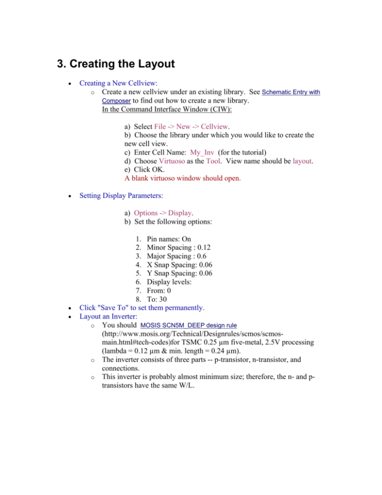
3. Creating the Layout • Creating a New Cellview: o Create a new cellview under an existing library. See Schematic Entry with Composer to find out how to create a new library. In the Command Interface Window (CIW): a) Select File -> New -> Cellview. b) Choose the library under which you would like to create the new cell view. c) Enter Cell Name: My_Inv (for the tutorial) d) Choose Virtuoso as the Tool. View name should be layout. e) Click OK. A blank virtuoso window should open. • Setting Display Parameters: a) Options -> Display. b) Set the following options: • • 1. Pin names: On 2. Minor Spacing : 0.12 3. Major Spacing : 0.6 4. X Snap Spacing: 0.06 5. Y Snap Spacing: 0.06 6. Display levels: 7. From: 0 8. To: 30 Click "Save To" to set them permanently. Layout an Inverter: o You should MOSIS SCN5M_DEEP design rule (http://www.mosis.org/Technical/Designrules/scmos/scmosmain.html#tech-codes)for TSMC 0.25 µm five-metal, 2.5V processing (lambda = 0.12 µm & min. length = 0.24 µm). o The inverter consists of three parts -- p-transistor, n-transistor, and connections. o This inverter is probably almost minimum size; therefore, the n- and ptransistors have the same W/L. o Layout of P-transistor with L=0.24 µm and W=0.48 µm. In this tutorial, we are using the Nwell process. Thus, the substrate will be p-substrate. We will create a pmos transistor first. To do that we need an Nwell in which the pmos transistor will be formed. Draw the well a) Select the n-well layer from the LSW window b) Select the Create->Rectangle (or choose the Rectangle icon from the side toolbar). c) Using your mouse, draw the n-well on the cellview to be 2.94 wide by 2.52 tall . Draw the p- and n-select regions for the p transistor a) Select the pselect layer from the LSW window; we will draw the pselect enclosing the transistor b) Select the Create->Rectangle (or choose the Rectangle icon from the side toolbar). c) Using your mouse, draw the pselect on the cellview; 1.98 wide and 0.96 tall; its left- and right-edges should be 0.48 away from well edges. The pselect should be placed within the n-well, even if the size should vary. (you can use the Edit->move command to move the layer) Draw Diffusions a) Select the pactive layer from the LSW window; we will draw the active region of the p-device b) Select the Create->Rectangle (or choose the Rectangle icon from the side toolbar). c) Using your mouse, draw the pactive on the cellview to be 1.5 wide by 0.48 tall - it should be enclosed by the pselect by 0.24 and by the nwell by at least 0.72 Draw Poly a) Select the poly layer from the LSW window b) Select the Create->Rectangle (or choose the Rectangle icon from the side toolbar). c) Using your mouse, draw the poly on the cellview to be 0.24 long by 1.32 wide. The poly should be placed at the center of the pisland. The poly should extend over the p-island by 0.30 um. Place Contacts a) Select the contact layer from the LSW window b) Select the Create->Rectangle (or choose the Rectangle icon from the side toolbar). c) Using your mouse, draw the contact on the cellview to be 0.24 long by 0.24 wide. The contact should be placed at both sides of the pactive. Repeat the above process for the second contact. o Layout of N-transistor with L=0.24 µm and W=0.48 µm. Draw the nselect a) Select the nselect layer from the LSW window b) Select the Create->Rectangle (or choose the Rectangle icon from the side toolbar). c) Using your mouse, draw the nselect on the cellview to be 1.98 wide by 0.92 tall Draw the N active region a) Select the nactive layer from the LSW window b) Select the Create->Rectangle (or choose the Rectangle icon from the side toolbar). c) Using your mouse, draw the nactive on the cellview to be 1.50 wide by 0.48 tall; it should be enclosed by the nselect by 0.24 around its edges. Also, it needs to be at least 0.72 away from the n-well (= 6 x lambda; MOSIS rule 2.3 for DEEP). Extend Poly a) Extend the poly layer created for the p-transistor over the n-island, making sure that the poly extension over nisland is 0.30. (you can use the Edit->Stretch command to stretch the poly) The poly should be placed at the center of the n-island. Place Contacts a) Select the contact layer from the LSW window b) Select the Create->Rectangle (or choose the Rectangle icon from the side toolbar). c) Using your mouse, draw the contact on the cellview to be 0.24 long by 0.24 wide. The contact should be placed at both sides of the pisland. Repeat the above process for the second contact. o Layout necessary connections Draw the well-contact a) Select the nselect layer from the LSW window; we will draw the nselect enclosing the substrate (vdd) contact for the P transistor. b) Select the Create->Rectangle (or choose the Rectangle icon from the side toolbar). c) Using the mouse, draw the nselect on the cellview; at least 0.96 tall and wide, as it will have to enclose the contact n-active by at least 0.24, which in turn enclose the contact by at least 0.12. The nselect abuts directly to the pselect of the P transistor, but they should not overlap. Also, both selects should be placed within the n-well. d) Select the nactive layer from the LSW window; we will draw the body contact region of the p device. e) Select the Create->Rectangle (or choose the Rectangle icon from the side toolbar). f) Using your mouse, draw the nactive on the cellview to be at least 0.48 wide by 0.48 tall g) Add a contact in the center of the well-contact island. Draw the Substrate-contact a) Select the pselect layer from the LSW window; we will draw the nselect enclosing the substrate (vss = ground) contact for the N transistor b) Select the Create->Rectangle (or choose the Rectangle icon from the side toolbar). c) Using the mouse, draw the pselect on the cellview; at least 0.96 tall and wide, as it will have to enclose the contact p-active by at least 0.24, which in turn enclose the contact by at least 0.12. The nselect abuts directly to the nselect of the N transistor, but they should not overlap. d) Select the pactive layer from the LSW window e) Select the Create->Rectangle (or choose the Rectangle icon from the side toolbar). f) Using your mouse, draw the n-island on the cellview to be 0.48 wide by 0.48 tall; it must be enclosed by the pselect by 0.24. The p-island should be placed at least 0.48 um (= 4 x lambda, MOSIS rule 2.5 DEEP) below the n-transistor. g) Add contacts in the center of the substrate-contact island. Metal Connections a) Connect the source of p-transistor to the well-contact using the metal 1 layer. b) Connect the source of n-transistor to the substratecontact using the metal 1 layer. c) Add a contact to the gate (poly) o Add Pins: You need to add pins for the input (named ip), output (named op), vdd, and vss in order to pass DRC. Creating I/O Pins Once you have finished creating the layout, the next step is to add the I/O pins of your circuit. It is necessary to add the vdd! and vss! connections to your circuit for the purpose of DRC. The following is a procedure to add I/O pins to your circuit: Before you start, you have to have a layout (view name: layout) in your library. o From your Layout window: 1. Choose Create->Pin... from the menu. The Create Pin form will appear. 2. If the form is titled "Create Shape Pin", choose "sym pin" under the Mode option. 3. Enter a TerminalName(the name of your pin). NOTE: For HSPICE, there is a node name limit of 16 characters. 4. Make sure that the "Display Pin Name" option is selected. 5. Specify the "I/O Type" as either input, output, or inputoutput. 6. Specify the Pin Type as either Metal1_T, Metal2_T,... depending on which is the top layer at the place that the pin is to be inserted. 7. Specify the Pin Width to the desired pin width (the pin is square). 8. Move the mouse to specify where the pin and the label should be placed. 9. Repeat the above process (1-7) for all the pins in your circuit. o Design Rule Check (DRC) DRC is used to check that all process-specific design rules (such as spacing) have been met. Design Rule Check (DRC) There are process-specific design rules that describe how close layers can be placed together and what the sizes of the areas can be. These rules are give the minimum requirement to avoid a catastrophic failure of your circuit due to fabrication faults. You can use the MOSIS SCMOS design rules (http://www.mosis.org/Technical/Designrules/scmos/scmos-main.html#tech-codes) as a guideline. The design rules are different for different processes. The following is a procedure to perform design rule check (DRC) for a layout. DRC outputs any violations of the design rules for your technology process. This step is important because the violation of any design rules would cause the fabricated chip to not function as desired. Before you start, you have to have a layout (view name: layout) in your library. o From your Layout window: 1. Choose Verify -> DRC from the menu. The Verify DRC form will appear. 2. Set the Switch Names field. This switch name depends on the process you're running. For the TSMC 0.25 um and other processes: Leave as default. 3. Click OK to run DRC. If your design has violated any design rules, DRC will reports the errors in the CIW. Errors are indicated by the markers (white color) on the circuit. You may then proceed to correcting the errors according to the design rules. 4. For huge layouts,the marker might not be easily located. To find markers, choose Verify -> Markers -> Find in layout window. A pop up menu will appear. Click on the Zoom to Markers box. Click on the Apply button and Cadence will zoom in to the errors or warnings as desired. The following commands are useful: command menu bar command shortcut create ruler Window - Create Ruler <k> delete all rulers Window - Clear All Rulers <K> zoom in Window - Zoom - In <z> Settings for the Virtuoso Layout XL Editor command menu bar command shortcut set the snap grid spacing Options - Display: set X Snap Spacing and Y <e> Snap Spacing to 0.025 set gravity on/off Options - Layout Editor: deselect Gravity On <E> show all levels of the devices Options - Display: Display Levels: From, To <SHIFT>-<f> show only single level of the devices <CTRL>-<f> Options - Display: Display Levels: From, To command menu bar command shortcut save the layout Design - Save <F2> zoom in Window - Zoom - In <z> fit complete layout in the layout window Window - Fit All <f> redraw layout window Window - Redraw <F6> create ruler Window - Create Ruler <k> delete all rulers Window - Clear All Rulers <K> undo last action Edit - Undo <u> move object Edit - Move <m> stretch object Edit - Stretch <s> delete object Edit - Delete <DEL> edit object properties Edit - Properties <q> terminate any command <ESC> rectangle Create - Rectangle <r> polygon Create - Polygon <P> path Create - Path <p> Layout creation - miscellaneous While placing components and routing, periodically start the Design-Rule-Check (DRC) in order to identify any violations of the design rules of the current process technology (min. spacing between geometries, min. width of geometries, ...). When implementing a standard cell it is also very important to consider the distances of geometries on the various layers to geometries in adjacent placed cells! These errors can't be found by the DRC of the single cell. The DRC will be explained in detail in the next section. If the schematic of the cell is changed during or after the cell has been layouted, the following commands could be of interest: command menu bar command change the nets at the terminals of Connectivity - Propagate Nets an instance update of components and nets Connectivity - Update Components And Nets
