EE 479 syllabus - University of Southern California
advertisement
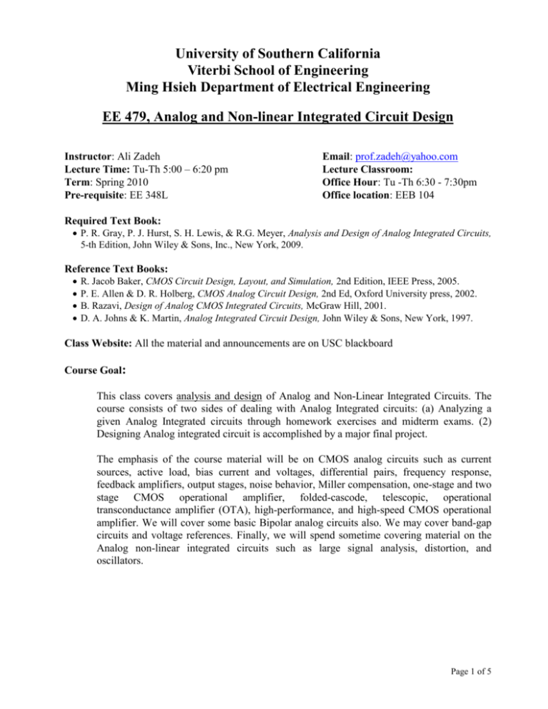
University of Southern California Viterbi School of Engineering Ming Hsieh Department of Electrical Engineering EE 479, Analog and Non-linear Integrated Circuit Design Instructor: Ali Zadeh Lecture Time: Tu-Th 5:00 – 6:20 pm Term: Spring 2010 Pre-requisite: EE 348L Email: prof.zadeh@yahoo.com Lecture Classroom: Office Hour: Tu -Th 6:30 - 7:30pm Office location: EEB 104 Required Text Book: P. R. Gray, P. J. Hurst, S. H. Lewis, & R.G. Meyer, Analysis and Design of Analog Integrated Circuits, 5-th Edition, John Wiley & Sons, Inc., New York, 2009. Reference Text Books: R. Jacob Baker, CMOS Circuit Design, Layout, and Simulation, 2nd Edition, IEEE Press, 2005. P. E. Allen & D. R. Holberg, CMOS Analog Circuit Design, 2nd Ed, Oxford University press, 2002. B. Razavi, Design of Analog CMOS Integrated Circuits, McGraw Hill, 2001. D. A. Johns & K. Martin, Analog Integrated Circuit Design, John Wiley & Sons, New York, 1997. Class Website: All the material and announcements are on USC blackboard Course Goal: This class covers analysis and design of Analog and Non-Linear Integrated Circuits. The course consists of two sides of dealing with Analog Integrated circuits: (a) Analyzing a given Analog Integrated circuits through homework exercises and midterm exams. (2) Designing Analog integrated circuit is accomplished by a major final project. The emphasis of the course material will be on CMOS analog circuits such as current sources, active load, bias current and voltages, differential pairs, frequency response, feedback amplifiers, output stages, noise behavior, Miller compensation, one-stage and two stage CMOS operational amplifier, folded-cascode, telescopic, operational transconductance amplifier (OTA), high-performance, and high-speed CMOS operational amplifier. We will cover some basic Bipolar analog circuits also. We may cover band-gap circuits and voltage references. Finally, we will spend sometime covering material on the Analog non-linear integrated circuits such as large signal analysis, distortion, and oscillators. Page 1 of 5 Grade: Final course grades are based on the following formula: Homework Assignments = 25% Midterm Exam = 25% Final Exam = 25% Class Project = 25% ================== = ======== Total = 100% Instructor’s Background: I am a part-time faculty in the Ming Hsieh Department of Electrical Engineering. I have many years of industrial experience in the design of Analog and Mixed-Signal Integrated circuits, Switched-Capacitor circuits and Filters, Analog-Digital Interface Integrated Circuits, Micro-power Biomedical Data-Converter Integrated Circuits and Systems, and CMOS Image sensors. 2008 – Now: St. Jude Medical Company, Principal Design Engineer. 2002 – 2008: Micron Technology, Inc., Image Sensor Design Manager. 1999 - 2002: Micro-semi Corporation, IC Design Manager. 1986 - 1999: St. Jude Medical Company, Senior Staff Scientist. 1982 - 1986: Harris Semiconductor, Senior Design Engineer. Exams There will two exams: one Midterm, one final exam. The dates of exams are announced in the class schedule. Final is NOT cumulative. Final exam covers only the material after midterm. Exams will be closed book. Students can bring one 8.5” x 11” page (both sides of the sheet) of notes for the midterms. The pages of notes must be hand written. Paper for exams will be supplied. Just bring a pen or a pencil, eraser, and a calculator. You must show how you derived the answers to the problems in order to receive full credit. Homework Assignments There will be six homework assignments given during the semester. Homework assignments will be given through the class web-site and are due by the announcements. If you cannot make it to the lecture, have a friend to turn in your homework for you. Homework and Project Report Policies: (1) Your homework must be professional quality work. (2) Use only standard 8.5 in x 11 in papers. (3) Use only one-side of each page. (4) Put stables on the upper-left corner. (5) Write nicely, large, neat and legibly. (6) Put each LTspice schematics and/or simulation results in separate pages. (7) Turn in your homework in the classroom at the beginning of the lecture. (8) Each person turns-in his/her homework individually. (9) Write your name precisely according to USC records: Last Name, First Name (10) Late homework and E-mail homework will NOT be accepted. Page 2 of 5 LTSpice Simulations We will be using LTSpice for simulations of our circuits, homework and project. LTSpice can be down-loaded free from Linear Technology, Inc. Website. It has schematic capture, simulations engine, and waveform view. LTSpice does NOT have any limitations on the number of transistors in your circuit schematic. We have model files for 0.18um (180nm) TSMC CMOS technology. This is Level 49 HSPICE (BSIM3v3) parameters, TSMC018.txt. This model file is from an actual processed wafer lot of TSMC provided by MOSIS. Taiwan Semiconductor Manufacturing Company (TSMC) is one of the leading and prominent providers of semiconductor wafers in the world. I will provide the model file and put them on the DEN Blackboard. You need to copy the text file in your PC and place it all in your simulation folder (the folder in which you have your circuit schematics and symbols). You need to include the model file in your schematic. You must become familiar to LTSpice in terms of: Schematic Capture, Creating SPICE Net-list, simulations, and viewing the waveform. I expect you to learn this as soon as possible. You need to become familiar with simulation tools within two weeks. Some simple circuit schematic will be provided and discussed in the class. (1) Use the following website to get all the information about LTSpice. http://cmosedu.com/cmos1/LTspice/LTspice.htm (2) To download the free LTSpice software, go to: http://www.linear.com/designtools/software/ (3) Several video instruction of how to use LTSpice is here: http://cmosedu.com/videos/LTspice/LTspice_videos.htm (4) LTspice User Manual is here: ltspice.linear.com/software/scad3.pdf Class Project One of the main purposes of the course is for student to have hands-on experience in designing a major CMOS Operational Amplifier integrated circuit using LTSpice Design Tools. Your project report must be professional quality work. Handwritten project will NOT be accepted. One or two persons can work on the same project. Page 3 of 5 The performance specification of the project operational amplifier is in Table 1. This opamp can be a part of high-speed data-converter circuit used in Imaging Sensor products. Parameter Description Required Achieved Value Priority Power Supply Voltage (Vdd) 1.8 1.8 V -------- Temperature (Room) 25 25 °C -------- Typical Typical ----- -------- 1 1 pF -------- TSMC 0.18um Process Corner Output Load Capacitor Opamp Open Loop DC Gain (Avo) > 100 dB Opamp Unity Gain-Bandwidth Product (UGBW) > 500 MHz 1 1 Phase Margin > 60 Degree 1 Settling Time (0.01% of 1V input step) <5 ns 1 V 1 > 0.75 Common-Mode Input Range Vin1-to-Vin2 =? Supply Current Consumption (Idd) < 25 mA 2 Power Consumption (Vdd X Idd) < 45 mW 2 Positive Slew Rate (SR+) >1 V/ns 2 Negative Slew Rate (SR-) >1 V/ns 2 Common Mode Rejection Ratio (at 100Hz) > 80 dB 3 Positive Power Supply Rejection Ratio (at 100Hz) > 60 dB 3 Negative Power Supply Rejection Ratio (at 100Hz) > 60 dB 3 Table 1. CMOS Operational Amplifier Specification for the project. Achieving all these specifications simultaneously will be challenging. Several papers and patents will be provided at the end of the semester to give you some ideas how to push the performance of your circuit. First try to achieve the minimum possible performance. Then, improve the opamp performance if you have additional time. The class project is graded based on: Organization and Project Report: Analysis and Hand Calculations: Circuit Design Innovation: Circuits /Test Circuit Diagrams: Graphs and Waveforms: Specification Performance: ======================= Total 10% 10% 10% 10% 10% 50% ====== 100% Page 4 of 5 EE 479 Weekly Schedule, Spring 2010 Week Tuesday Lecture Thursday Lecture (1) Syllabus, Introduction, Analog vs. digital world, MOS Technology trends, Low-voltage Mixed-signal PN Junction, depletion region, Build-in potential, Junction capacitance, MOS device cross section and layout. MOS Device, Small signal equivalent, DC bias and MOS low-Frequency ac equivalent models MOS high-frequency model, MOS capacitances, Gate Capacitances and Junction Capacitances, fT freq Three Basic Configurations: Common source (CS) amplifier, Common-Gate, and Source Follower (SF) Config. MOS Second order effects, Early Voltage, Body effect, Weak vs. Strong Inversion Differential pairs, Differential mode vs. common mode gain, common mode rejection ratio. Active loads, Differential pair with active current mirror load, CommonMode Rejection Ratio. Simple Current source, Cascode current source, Wilson current course, Low-voltage Sooch current source One-stage amplifiers, Telescopic, Folded Cascode, Operational trans-conductance amplifier (OTA) Voltage and current references, Self biasing VT reference, CMOS VT Reference. Operational amplifier with single-ended output, Op-amp application, CMRR, PSRR+, PSRR-, Common-Mode input Range 01/12 - 01/14 (2) 01/19 - 01/21 (3) 01/26 - 01/28 (4) 02/02 - 02/04 (5) 02/09 - 02/011 (6) 02/16 – 02/18 (7) 02/23 – 02/25 (8) 03/02 – 03/04 Midterm Review Bipolar Transistor, npn and pnp devices, Bipolar transconductance, BJT Small signal AC equivalent Cascade and cascade configuration Gain enhancement, CS amplifier with source degeneration. Assignments Chapter 1 LTSpice Setup LTSpice Videos Chapter 2 Chapter 3 Chapter 3 Chapter 4 Chapter 4 Chapter 6 Midterm Exam (March 4) Chapters: 1, 2, 3, 4 Continuous and Switched-Capacitor amplifiers, Two-stage MOS Op-amp with cascodes Telescopic and MOS folded cascade operational amplifiers. Operational transconcutance amplifiers Chapter 6 Frequency response for high-pass, low-pass poles and zeros, Magnitude and Phase response, Bode plot. Frequency response of Three basic Configurations: CS, CG, SF amplifiers Chapter 7 Feedback , Effect of negative feedback, Feedback loop gain, feed forward, Return ratio analysis Amplifier feedback, first order model, Gainbandwidth trade-off, frequency vs. transient response. Chapter 8 Damping ratio , natural frequency, Phase Margin, Settling time, Peak-overshoot ratio, 04/20 – 04/22 Amplifier feedback, Second order model, Gain-bandwidth trade-off, frequency vs. transient response. Compensation, One-stage opamap, Miller effect, two-stage opamp, Polesplitting, Right-half-plan zero Large signal analysis of Analog circuits and MOS amplifiers, Distortion analysis. (15) Final Review Final Exam (April 29) Chapters: 6, 7, 8, 9 Final Project Due: Monday, May 10 @ 6pm (9) 03/09 – 03/11 (10) 03/23 – 03/25 (11) 03/30 – 04/01 (12) 04/06 – 04/08 (13) 04/13 – 04/15 (14) 04/27 – 04/29 Complete Two-stage operational amplifier analysis, Slew-rate, Small signal vs., large signal, RHP zero elimination. MOS Crystal’s oscillator. Loop gain, frequency response, low-power crystal oscillators Chapter 9 Chapter 9 Notes Page 5 of 5
